参数资料
| 型号: | HFA1135IBZ |
| 厂商: | Intersil |
| 文件页数: | 13/15页 |
| 文件大小: | 0K |
| 描述: | IC OPAMP CFA 360MHZ LP 8-SOIC |
| 标准包装: | 98 |
| 应用: | 电流反馈 |
| 电路数: | 1 |
| -3db带宽: | 360MHz |
| 转换速率: | 1530 V/µs |
| 电流 - 电源: | 6.9mA |
| 电流 - 输出 / 通道: | 60mA |
| 电压 - 电源,单路/双路(±): | ±4.5 V ~ 5.5 V |
| 安装类型: | 表面贴装 |
| 封装/外壳: | 8-SOIC(0.154",3.90mm 宽) |
| 供应商设备封装: | 8-SOIC |
| 包装: | 管件 |
| 产品目录页面: | 1234 (CN2011-ZH PDF) |
7
When the output is limited, the negative input continues to
source a slewing current (ILIMIT) in an attempt to force the
output to the quiescent voltage defined by the input. QP5
must sink this current while limiting, because the -IN current
is always mirrored onto the high impedance node. The
limiting current is calculated as:
ILIMIT = (V-IN - VOUT LIMITED)/RF + V-IN/RG.
As an example, a unity gain circuit with VIN = 2V, and VH =1V,
would have ILIMIT = (2V - 1V)/1.5k +2V/∞ = 667A (RG = ∞
for unity gain applications). Note that ICC increases by ILIMIT
when the output is limited.
Limit Accuracy
The limited output voltage will not be exactly equal to the
voltage applied to VH or VL. Offset errors, mostly due to VBE
mismatches, necessitate a limit accuracy parameter which is
found in the device specifications. Limit accuracy is a
function of the limiting conditions. Referring again to Figure
3, it can be seen that one component of limit accuracy is the
VBE mismatch between the QX6 transistors, and the QX5
transistors. If the transistors always ran at the same current
level there would be no VBE mismatch, and no contribution
to the inaccuracy. The QX6 transistors are biased at a
constant current, but as described earlier, the current
through QX5 is equivalent to ILIMIT. VBE increases as ILIMIT
increases, causing the limited output voltage to increase as
well. ILIMIT is a function of the overdrive level
((AV xVIN -VLIMIT) / VLIMIT), so limit accuracy degrades as
the overdrive increases. For example, accuracy degrades
from +15mV to +70mV when the overdrive increases from
100% to 200% (AV = +2, VH = 500mV, RF =250).
Consideration must also be given to the fact that the limit
voltages have an effect on amplifier linearity. The “Linearity
Near Limit Voltage” curves, Figures 34 and 35, illustrate the
impact of several limit levels on linearity.
Limit Range
Unlike some competitor devices, both VH and VL have usable
ranges that cross 0V. While VH must be more positive than
VL, both may be positive or negative, within the range
restrictions indicated in the specifications. For example, the
HFA1135 could be limited to ECL output levels by setting
VH = -0.8V and VL = -1.8V. VH and VL may be connected to
the same voltage (GND for instance) but the result won’t be a
DC output voltage from an AC input signal. A 150mV - 200mV
AC signal will still be present at the output.
Recovery from Overdrive
The output voltage remains at the limit level as long as the
overdrive condition remains. When the input voltage drops
below the overdrive level (VLIMIT/AV) the amplifier returns to
linear operation. A time delay, known as the Overdrive
Recovery Time, is required for this resumption of linear
operation. Overdrive recovery time is defined as the
difference between the amplifier’s propagation delay exiting
limiting and the amplifier’s normal propagation delay, and it is
a strong function of the overdrive level. Figure 36 details the
overdrive recovery time for various limit and overdrive levels.
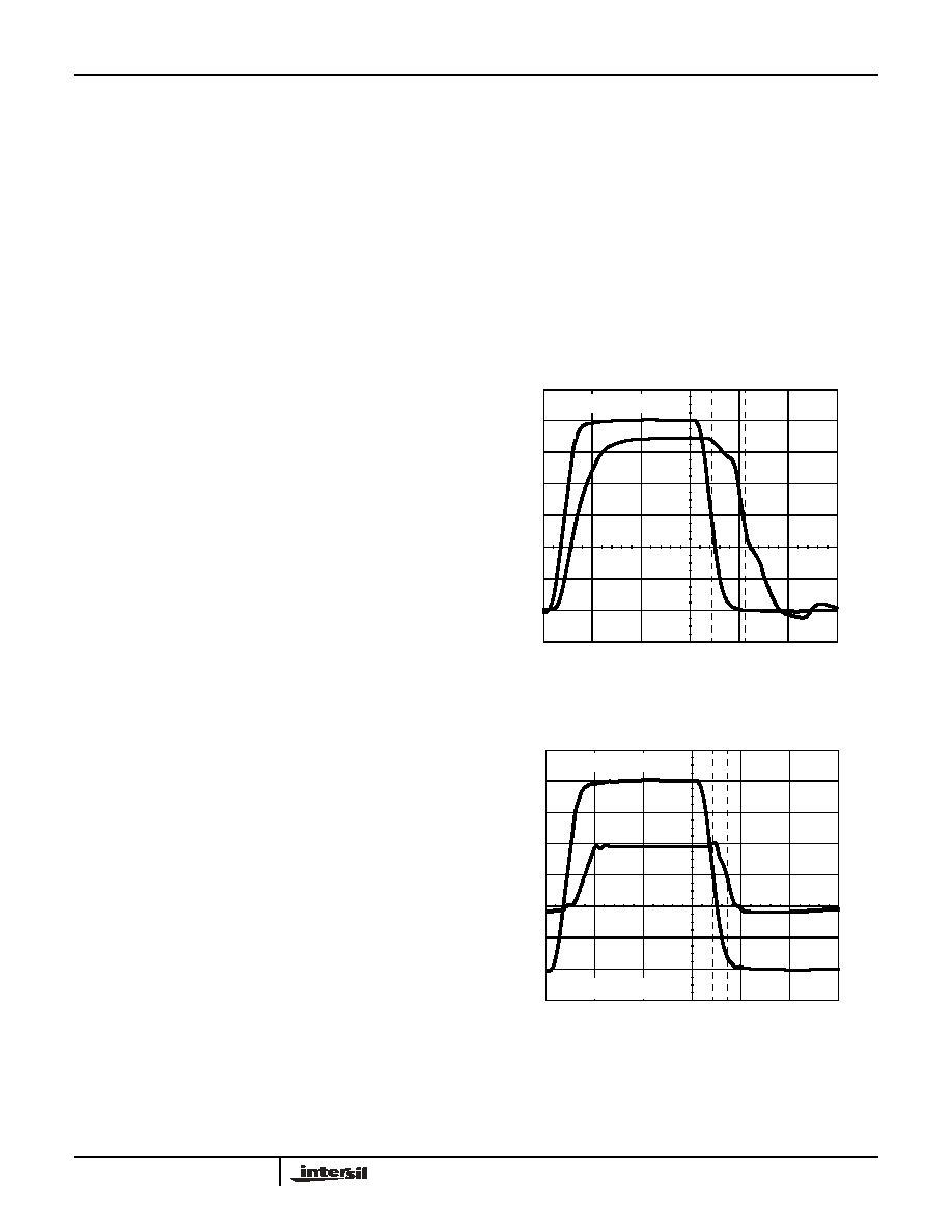
Benefits of Output Limiting
The plots of “Pulse Response Without Limiting” and “Pulse
Response With Limiting” (Figures 4 and 5) highlight the
advantages of output limiting. Besides the obvious benefit of
constraining the output swing to a defined range, limiting the
output excursions also keeps the output transistors from
saturating, which prevents unwanted saturation artifacts
from distorting the output signal. Output limiting also takes
advantage of the HFA1135’s ultra-fast overdrive recovery
time, reducing the recovery time from 2.3ns to 0.3ns, based
on the amplifier’s normal propagation delay of 1.2ns.
FIGURE 4. PULSE RESPONSE WITHOUT LIMITING
FIGURE 5. PULSE RESPONSE WITH LIMITING
TIME (5ns/DIV.)
INP
U
T
V
O
L
T
A
G
E
(V
)
AV = +2, RF = 250
0
OUT
-0.5
-1.0
0.5
1.0
1.5
2.0
OUT
P
UT
V
O
L
T
A
G
E
(V)
0
-1.0
-2.0
1.0
2.0
3.0
4.0
IN
TIME (5ns/DIV.)
INPUT
V
O
L
T
A
G
E
(V
)
AV = +2, RF = 250
0
OUT
VH = +2.0V, VL = 0V
0.5
1.0
-0.5
IN
OUT
P
UT
V
O
L
T
A
G
E
(V
)
0
1.0
2.0
-1.0
1.5
2.0
HFA1135
相关PDF资料 |
PDF描述 |
|---|---|
| LTC2754BIUKG-16#TRPBF | IC DAC 16BIT QUAD IOUT 52-QFN |
| HA3-5020-5Z | IC AMP VIDEO CFA 100MHZ 8-DIP |
| HFA1105IBZ | IC OPAMP CFA 330MHZ LP 8-SOIC |
| VI-B1N-MU | CONVERTER MOD DC/DC 18.5V 200W |
| HA9P5020-5Z | IC AMP VIDEO 100MHZ CFB 8-SOIC |
相关代理商/技术参数 |
参数描述 |
|---|---|
| HFA1135IBZ | 制造商:Intersil Corporation 功能描述:IC VIDEO OP AMP 360MHZ |
| HFA1135IBZ96 | 功能描述:视频放大器 W/ANNEAL OPAMP 360MHZ CFB LIMIT IND RoHS:否 制造商:ON Semiconductor 通道数量:4 电源类型: 工作电源电压:3.3 V, 5 V 电源电流: 最小工作温度: 最大工作温度: 封装 / 箱体:TSSOP-14 封装:Reel |
| HFA1135MJ/883 | 制造商:Rochester Electronics LLC 功能描述:- Bulk |
| HFA1135ML/883 | 制造商:Rochester Electronics LLC 功能描述:- Bulk |
| HFA113MJ/883 | 制造商:Harris Corporation 功能描述: |
发布紧急采购,3分钟左右您将得到回复。