- 您现在的位置:买卖IC网 > PDF目录385375 > HFA1212 (Intersil Corporation) Dual 350MHz, Low Power Closed Loop Buffer Amplifier(350MHz、低功耗、输出限定锁相环缓冲器放大器) PDF资料下载
参数资料
| 型号: | HFA1212 |
| 厂商: | Intersil Corporation |
| 英文描述: | Dual 350MHz, Low Power Closed Loop Buffer Amplifier(350MHz、低功耗、输出限定锁相环缓冲器放大器) |
| 中文描述: | 双350MHz的低功耗闭环缓冲放大器(350MHz频段,低功耗,输出限定锁相环缓冲器放大器) |
| 文件页数: | 4/10页 |
| 文件大小: | 90K |
| 代理商: | HFA1212 |
4
Application Information
HFA1212 Advantages
The HFA1212 features a novel design which allows the user
to select from three closed loop gains, without any external
components. The result is a more flexible product, fewer part
types in inventory, and more efficient use of board space.
Implementing a dual, gain of 2, cable driver with this IC
eliminates the four gain setting resistors, which frees up
board space for termination resistors.
Likemostnewerhighperformanceamplifiers,theHFA1212isa
current feedback amplifier (CFA). CFAs offer high bandwidth
and slew rate at low supply currents, but can be difficult to use
because of their sensitivity to feedback capacitance and
parasitics onthe inverting input (summing node). The HFA1212
eliminates these concerns by bringing the gain setting resistors
on-chip. This yields the optimum placement and value of the
feedback resistor, while minimizing feedback and summing
node parasitics. Because there is no access to the summing
node, the PCB parasitics do not impact performance at gains of
+2 or -1 (see “Unity Gain Considerations” for discussion of
parasitic impact on unity gain performance).
The HFA1212’s closed loop gain implementation provides
better gain accuracy, lower offset and output impedance,
and better distortion compared with open loop buffers.
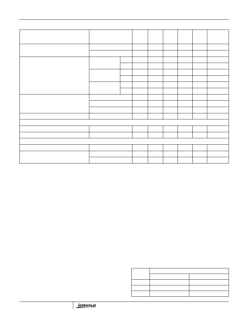
Closed Loop Gain Selection
This “buffer” operates in closed loop gains of -1, +1, or +2, with
gain selection accomplished via connections to the inputs
Applying the input signal to +IN and floating -IN selects a gain
of +1 (see next section for layout caveats), while grounding -IN
selects a gain of +2. A gain of -1 is obtained by applying the
input signal to -IN with +IN grounded through a 50
resistor.
The table below summarizes these connections:
Overshoot
(V
OUT
= 0.5V
P-P
, V
IN
t
RISE
= 1ns, Note 5)
+OS
B
25
-
4
-
%
-OS
B
25
-
13
-
%
Slew Rate
(V
OUT
= 5V
P-P
at A
V
= +2 or -1,
V
OUT
= 4V
P-P
at A
V
= +1)
A
V
= -1
+SR
B
25
-
2000
-
V/
μ
s
-SR
B
25
-
1150
-
V/
μ
s
A
V
= +1,
+R
S
= 620
+SR
B
25
-
1100
-
V/
μ
s
-SR
B
25
-
850
-
V/
μ
s
A
V
= +2
+SR
B
25
-
1300
-
V/
μ
s
-SR
B
25
-
900
-
V/
μ
s
Settling Time
(V
OUT
= +2V to 0V Step, Note 4)
To 0.1%
B
25
-
24
-
ns
To 0.05%
B
25
-
37
-
ns
To 0.02%
B
25
-
60
-
ns
Overdrive Recovery Time
V
IN
=
±
2V
B
25
-
8.5
-
ns
VIDEO CHARACTERISTICS
Differential Gain (f = 3.58MHz, A
V
= +2)
R
L
= 150
R
L
= 150
B
25
-
0.025
-
%
Differential Phase (f = 3.58MHz, A
V
= +2)
B
25
-
0.03
-
Degrees
POWER SUPPLY CHARACTERISTICS
Power Supply Range
C
25
±
4.5
-
±
5.5
V
Power Supply Current
A
25
-
5.9
6.1
mA/Op Amp
A
Full
-
6.1
6.3
mA/Op Amp
NOTES:
3. Test Level: A. Production Tested; B. Typical or Guaranteed Limit Based on Characterization; C. Design Typical for Information Only.
4. See Typical Performance Curves for more information.
5. Negative overshoot dominates for output signal swings below GND (e.g. 0.5V
P-P
), yielding a higher overshoot limit compared to the
V
OUT
= 0V to 0.5V condition. See the “Application Information” section for details.
Electrical Specifications
V
SUPPLY
=
±
5V, A
V
= +1, R
L
= 100
,
Unless Otherwise Specified.
(Continued)
PARAMETER
TEST
CONDITIONS
(NOTE 3)
TEST
LEVEL
TEMP
(
o
C)
MIN
TYP
MAX
UNITS
GAIN
(A
CL
)
-1
CONNECTIONS
+INPUT
50
to GND
Input
-INPUT
Input
+1
NC (Floating)
+2
Input
GND
HFA1212
相关PDF资料 |
PDF描述 |
|---|---|
| HFA1245IP | XC95216-10PQ160C - NOT RECOMMENDED for NEW DESIGN |
| HFA1245 | Dual, 420MHz, Low Power, Video, Current Feedback Operational Amplifier with Disable(双路、420MHz低功耗、电流反馈视频运算放大器) |
| HFA1305IB | Circular Connector; No. of Contacts:55; Series:; Body Material:Aluminum; Connecting Termination:Solder; Connector Shell Size:22; Circular Contact Gender:Pin; Circular Shell Style:Straight Plug; Insert Arrangement:22-55 |
| HFA1405IP | Quad, 560MHz, Low Power, Video Operational Amplifier |
| HFA1405IB | Circular Connector; Body Material:Aluminum; Series:PT06; No. of Contacts:55; Connector Shell Size:22; Connecting Termination:Solder; Circular Shell Style:Straight Plug; Circular Contact Gender:Pin; Insert Arrangement:22-55 |
相关代理商/技术参数 |
参数描述 |
|---|---|
| HFA1212/883 | 制造商:INTERSIL 制造商全称:Intersil Corporation 功能描述:Dual, High Speed, Low Power, Video Closed Loop Buffer |
| HFA1212_04 | 制造商:INTERSIL 制造商全称:Intersil Corporation 功能描述:Dual 350MHz, Low Power Closed Loop Buffer Amplifier |
| HFA1212883 | 制造商:INTERSIL 制造商全称:Intersil Corporation 功能描述:Dual, High Speed, Low Power, Video Closed Loop Buffer |
| HFA1212IB | 制造商:INTERSIL 制造商全称:Intersil Corporation 功能描述:Dual 350MHz, Low Power Closed Loop Buffer Amplifier |
| HFA1212IP | 制造商:Rochester Electronics LLC 功能描述:BUFFER 2X 350MHZ PROG GAIN 8PDIP IND - Bulk |
发布紧急采购,3分钟左右您将得到回复。