- 您现在的位置:买卖IC网 > PDF目录385375 > HFA1212 (Intersil Corporation) Dual 350MHz, Low Power Closed Loop Buffer Amplifier(350MHz、低功耗、输出限定锁相环缓冲器放大器) PDF资料下载
参数资料
| 型号: | HFA1212 |
| 厂商: | Intersil Corporation |
| 英文描述: | Dual 350MHz, Low Power Closed Loop Buffer Amplifier(350MHz、低功耗、输出限定锁相环缓冲器放大器) |
| 中文描述: | 双350MHz的低功耗闭环缓冲放大器(350MHz频段,低功耗,输出限定锁相环缓冲器放大器) |
| 文件页数: | 5/10页 |
| 文件大小: | 90K |
| 代理商: | HFA1212 |
5
Unity Gain Considerations
Unity gain selection is accomplished by floating the -Input of
the HFA1212. Anything that tends to short the -Input to GND,
such as stray capacitance at high frequencies, will cause the
amplifier gain to increase toward a gain of +2. The result is
excessive high frequency peaking, and possible instability.
Even the minimal amount of capacitance associated with
attaching the -Input lead to the PCB results in approximately
6dB of gain peaking. At a minimum this requires due care to
ensure the minimum capacitance at the -Input connection.
Table 1 lists five alternate methods for configuring the HFA1212
as a unity gain buffer, and the corresponding performance. The
implementations vary in complexity and involve performance
trade-offs. The easiest approach to implement is simply
shorting the two input pins together, and applying the input
signal to this common node. The amplifier bandwidth
decreasesfrom430MHzto280MHz,butexcellentgainflatness
is the benefit. A drawback to this approach is that the amplifier
input noise voltage and input offset voltage terms see a gain of
+2, resulting in higher noise and output offset voltages.
Alternately, a 100pF capacitor between the inputs shorts them
only at high frequencies, which prevents the increased output
offset voltage but delivers less gain flatness.
Another straightforward approach is to add a 620
resistor
in series with the amplifier’s positive input. This resistor and
the HFA1212 input capacitance form a low pass filter which
rolls off the signal bandwidth before gain peaking occurs.
This configuration was employed to obtain the data sheet AC
and transient parameters for a gain of +1.
Pulse Overshoot
The HFA1212 utilizes a quasi-complementary output stage to
achieve high output current while minimizing quiescent supply
current. In this approach, a composite device replaces the
traditional PNP pulldown transistor. The composite device
switches modes after crossing 0V, resulting in added distortion
for signals swinging below ground, and an increased overshoot
on the negative portion of the output waveform (see Figure 6,
Figure 9, and Figure 12). This overshoot isn’t present for small
bipolar signals (see Figure 4, Figure 7, and Figure 10) or large
positive signals (see Figure 5, Figure 8 and Figure 11).
PC Board Layout
This amplifier’s frequency response depends greatly on the
care taken in designing the PC board (PCB).
The use of low
inductance components such as chip resistors and chip
capacitors is strongly recommended, while a solid
ground plane is a must!
Attention should be given to decoupling the power supplies.
A large value (10
μ
F) tantalum in parallel with a small value
(0.1
μ
F) chip capacitor works well in most cases.
Terminated microstrip signal lines are recommended at the
input and output of the device. Capacitance directly on the
output must be minimized, or isolated as discussed in the
next section.
An example of a good high frequency layout is the
Evaluation Board shown in Figure 3.
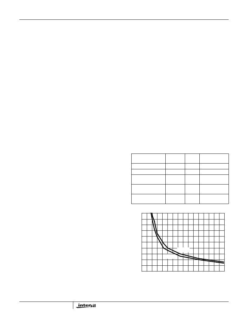
Driving Capacitive Loads
Capacitive loads, such as an A/D input, or an improperly
terminated transmission line will degrade the amplifier’s
phase margin resulting in frequency response peaking and
possible oscillations. In most cases, the oscillation can be
avoided by placing a resistor (R
S
) in series with the output
prior to the capacitance.
Figure 1 details starting points for the selection of this
resistor. The points on the curve indicate the R
S
and C
L
combinations for the optimum bandwidth, stability, and
settling time, but experimental fine tuning is recommended.
Picking a point above or to the right of the curve yields an
overdamped response, while points below or left of the curve
indicate areas of underdamped performance.
R
S
and C
L
form a low pass network at the output, thus
limiting system bandwidth well below the amplifier bandwidth
of 350MHz. By decreasing R
S
as C
L
increases (as
illustrated in the curves), the maximum bandwidth is
obtained without sacrificing stability. In spite of this,
bandwidth decreases as the load capacitance increases.
TABLE 1. UNITY GAIN PERFORMANCE FOR VARIOUS
IMPLEMENTATIONS
APPROACH
PEAKING
(dB)
BW
(MHz)
±
0.1dB GAIN
FLATNESS (MHz)
Remove -IN Pin
4.5
430
21
+R
S
= 620
+R
S
= 620
and
Remove -IN Pin
0
220
27
0.5
215
15
Short +IN to -IN (e.g.,
Pins 2 and 3)
0.6
280
70
100pF Capacitor
Between +IN and -IN
0.7
290
40
0
100
200
300
400
0
10
20
30
40
50
LOAD CAPACITANCE (pF)
S
)
A
V
= +2
150
250
350
50
A
V
= +1
FIGURE 1. RECOMMENDED SERIES RESISTOR vs LOAD
CAPACITANCE
HFA1212
相关PDF资料 |
PDF描述 |
|---|---|
| HFA1245IP | XC95216-10PQ160C - NOT RECOMMENDED for NEW DESIGN |
| HFA1245 | Dual, 420MHz, Low Power, Video, Current Feedback Operational Amplifier with Disable(双路、420MHz低功耗、电流反馈视频运算放大器) |
| HFA1305IB | Circular Connector; No. of Contacts:55; Series:; Body Material:Aluminum; Connecting Termination:Solder; Connector Shell Size:22; Circular Contact Gender:Pin; Circular Shell Style:Straight Plug; Insert Arrangement:22-55 |
| HFA1405IP | Quad, 560MHz, Low Power, Video Operational Amplifier |
| HFA1405IB | Circular Connector; Body Material:Aluminum; Series:PT06; No. of Contacts:55; Connector Shell Size:22; Connecting Termination:Solder; Circular Shell Style:Straight Plug; Circular Contact Gender:Pin; Insert Arrangement:22-55 |
相关代理商/技术参数 |
参数描述 |
|---|---|
| HFA1212/883 | 制造商:INTERSIL 制造商全称:Intersil Corporation 功能描述:Dual, High Speed, Low Power, Video Closed Loop Buffer |
| HFA1212_04 | 制造商:INTERSIL 制造商全称:Intersil Corporation 功能描述:Dual 350MHz, Low Power Closed Loop Buffer Amplifier |
| HFA1212883 | 制造商:INTERSIL 制造商全称:Intersil Corporation 功能描述:Dual, High Speed, Low Power, Video Closed Loop Buffer |
| HFA1212IB | 制造商:INTERSIL 制造商全称:Intersil Corporation 功能描述:Dual 350MHz, Low Power Closed Loop Buffer Amplifier |
| HFA1212IP | 制造商:Rochester Electronics LLC 功能描述:BUFFER 2X 350MHZ PROG GAIN 8PDIP IND - Bulk |
发布紧急采购,3分钟左右您将得到回复。