参数资料
| 型号: | HI1-574AKD-5 |
| 厂商: | Intersil |
| 文件页数: | 4/18页 |
| 文件大小: | 0K |
| 描述: | IC ADC 12BIT 40KSPS 1CH 28-SBDIP |
| 标准包装: | 78 |
| 位数: | 12 |
| 采样率(每秒): | 40k |
| 数据接口: | 并联 |
| 转换器数目: | 1 |
| 功率耗散(最大): | 720mW |
| 电压电源: | 双 ± |
| 工作温度: | 0°C ~ 75°C |
| 安装类型: | 通孔 |
| 封装/外壳: | 28-CDIP(0.600",15.24mm) |
| 供应商设备封装: | 28-CDIP |
| 包装: | 管件 |
| 输入数目和类型: | 2 个单端,单极;2 个单端,双极 |
12
FN3096.6
August 7, 2008
required, either or both pots may be replaced by a 50
Ω, 1%
metal film resistor.
Connect the Analog signal to pin 13 for a
±5V range, or to
pin 14 for a
±10V range. Calibration of offset and gain is
similar to that for the unipolar ranges as discussed above.
First apply a DC input voltage 1/2 LSB above negative full
scale (i.e., -4.9988V for the
±5V range, or -9.9976V for the
±10V range). Adjust the offset potentiometer R1 for flicker
between output codes 0000 0000 0000 and 0000 0000
0001. Next, apply a DC input voltage 11/2 LSBs below
positive full scale (+4.9963V for
±5V range; +9.9927V for
±10V range). Adjust the Gain potentiometer R2 for flicker
between codes 1111 1111 1110 and 1111 1111 1111.
NOTE: The 100
Ω potentiometer R2 provides Gain Adjust for the 10V
and 20V ranges. In some applications, a full scale of 10.24V (LSB
equals 2.5mV) or 20.48V (LSB equals 5.0mV) is more convenient.
For these, replace R2 by a 50
Ω, 1% metal film resistor. Then, to pro-
vide Gain Adjust for the 10.24V range, add a 200
Ω potentiometer in
series with pin 13. For the 20.48V range, add a 500
Ω potentiometer
in series with pin 14.
Controlling the HI-X74A
The HI-X74A includes logic for direct interface to most
microprocessor systems. The processor may take full
control of each conversion, or the converter may operate in
the “stand-alone” mode, controlled only by the R/C input.
Full control consists of selecting an 8-bit or 12-bit
conversion cycle, initiating the conversion, and reading the
output data when ready-choosing either 12 bits at once or 8
followed by 4, in a left-justified format. The five control
inputs are all TTL/CMOS-compatible: (12/8, CS, AO, R/C
and CE). Table 3 illustrates the use of these inputs in
controlling the converter’s operations. Also, a simplified
schematic of the internal control logic is shown in Figure 6.
“Stand-Alone Operation”
The simplest control interface calls for a single control line
connected to R/C. Also, CE and 12/8 are wired high, CS and
AO are wired low, and the output data appears in words of
12 bits each.
The R/C signal may have any duty cycle within (and
general, data may be read when R/C is high unless STS is
also high, indicating a conversion is in progress. Timing
parameters particular to this mode of operation are listed in
Conversion Length
A Convert Start transition (see Table 1) latches the state of
AO, which determines whether the conversion continues for
12 bits (AO low) or stops with 8 bits (AO high). If all 12 bits are
read following an 8-bit conversion, the last three LSBs will
read ZERO and DB3 will read ONE. AO is latched because it
is also involved in enabling the output buffers (see ““Reading
the Output Data” on page 13). No other control inputs are
latched.
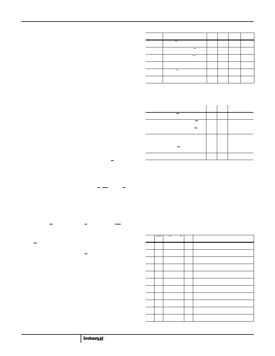
TABLE 1. HI-574A STAND-ALONE MODE TIMING
SYMBOL
PARAMETER
MIN
TYP
MAX
UNITS
tHRL
Low R/C Pulse Width
50
-
ns
tDS
STS Delay from R/C
-
200
ns
tHDR
Data Valid after R/C Low
25
-
ns
tHS
STS Delay after Data Valid 300
-
1200
ns
tHRH
High R/C Pulse Width
150
-
ns
tDDR
Data Access Time
-
150
ns
Time is measured from 50% level of digital transitions. Tested with a
50pF and 3k
Ω load.
TABLE 2. HI-674A STAND-ALONE MODE TIMING
SYMBOL
PARAMETER
MIN
TYP
MAX
UNITS
tHRL
Low R/C Pulse Width
50
-
ns
tDS
STS Delay from R/C
-
200
ns
tHDR
Data Valid after R/C Low
25
-
ns
tHS
STS Delay after Data
Valid
25
-
850
ns
tHRH
High R/C Pulse Width
150
-
ns
tDDR
Data Access Time
-
150
ns
Time is measured from 50% level of digital transitions. Tested with
a 50pF and 3k
Ω load.
TABLE 3. TRUTH TABLE FOR HI-X74A CONTROL INPUTS
CE
CS
R/C
12/8
AO
OPERATION
0
X
None
X
1
X
None
↑
0
X
0
Initiate 12-bit conversion
↑
0
X
1
Initiate 8-bit conversion
1
↓
0
X
0
Initiate 12-bit conversion
1
↓
0
X
1
Initiate 8-bit conversion
10
↓
X
0
Initiate 12-bit conversion
10
↓
X
1
Initiate 8-bit conversion
1
0
1
X
Enable 12-bit Output
1
0
1
0
Enable 8 MSBs Only
1
0
1
0
1
Enable 4 LSBs Plus 4 Trailing Zeroes
HI-574A, HI-674A
相关PDF资料 |
PDF描述 |
|---|---|
| VE-21N-MX-F4 | CONVERTER MOD DC/DC 18.5V 75W |
| MAX11666AUB/V+T | IC ADC 12BIT SRL 500KSPS 10UMAX |
| MS27473T14B15P | CONN PLUG 15POS STRAIGHT W/PINS |
| IDT72605L20PF8 | IC FIFO BI SYNC 256X18 64-TQFP |
| MAX11613EWC+T | IC ADC SERIAL 12BIT 4CH 12WLP |
相关代理商/技术参数 |
参数描述 |
|---|---|
| HI1-574AKDB3924-0003 | 制造商:Rochester Electronics LLC 功能描述:- Bulk 制造商:Harris Corporation 功能描述: |
| HI1-574ALD5 | 制造商:未知厂家 制造商全称:未知厂家 功能描述:Converter IC |
| HI1-574ALD-5 | 制造商:Rochester Electronics LLC 功能描述:- Bulk |
| HI1-574ASAD/883 | 制造商:Rochester Electronics LLC 功能描述:- Bulk |
| HI1-574ASD/883 | 制造商:Rochester Electronics LLC 功能描述:ADC 12BIT 50KSPS 28SBDIP /883 - Bulk |
发布紧急采购,3分钟左右您将得到回复。