参数资料
| 型号: | HI1-574AKD-5 |
| 厂商: | Intersil |
| 文件页数: | 5/18页 |
| 文件大小: | 0K |
| 描述: | IC ADC 12BIT 40KSPS 1CH 28-SBDIP |
| 标准包装: | 78 |
| 位数: | 12 |
| 采样率(每秒): | 40k |
| 数据接口: | 并联 |
| 转换器数目: | 1 |
| 功率耗散(最大): | 720mW |
| 电压电源: | 双 ± |
| 工作温度: | 0°C ~ 75°C |
| 安装类型: | 通孔 |
| 封装/外壳: | 28-CDIP(0.600",15.24mm) |
| 供应商设备封装: | 28-CDIP |
| 包装: | 管件 |
| 输入数目和类型: | 2 个单端,单极;2 个单端,双极 |
13
FN3096.6
August 7, 2008
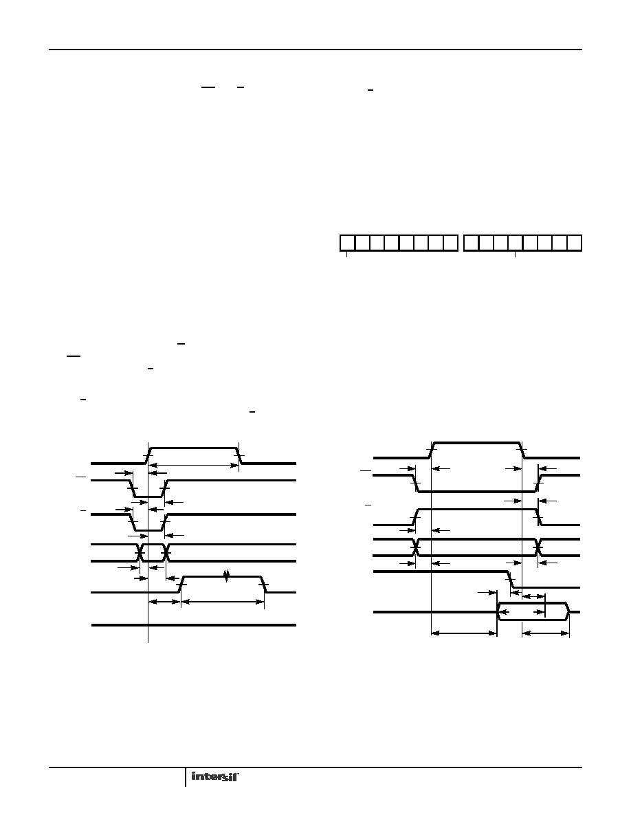
Conversion Start
A conversion may be initiated as shown in Table 3 by a logic
transition on any of three inputs: CE, CS or R/C. The last of
the three to reach the correct state starts the conversion, so
one, two or all three may be dynamically controlled. The
nominal delay from each is the same, and if necessary, all
three may change state simultaneously. However, to ensure
that a particular input controls the start of conversion, the
other two should be set up at least 50ns earlier. See the
HI-X74A Timing Specifications, Convert Mode.
This variety of HI-X74A control modes allows a simple
interface in most system applications. The Convert Start
timing relationships are illustrated in Figure 3.
The output signal STS indicates status of the converter by
going high only while a conversion is in progress. While STS
is high, the output buffers remain in a high impedance state
and data cannot be read. Also, an additional Start Convert
will not reset the converter or re-initiate a conversion while
STS is high.
Reading the Output Data
The output data buffers remain in a high impedance state
until four conditions are met: R/C high, STS low, CE high
and CS low. At that time, data lines become active according
to the state of inputs 12/8 and AO. Timing constraints are
illustrated in Figure 4.
The 12/8 input will be tied high or low in most applications,
though it is fully TTL/CMOS-compatible. With 12/8 high, all
12 output lines become active simultaneously, for interface
to a 12-bit or 16-bit data bus. The AO input is ignored.
With 12/8 low, the output is organized in two 8-bit bytes,
selected one at a time by AO. This allows an 8-bit data bus
the least significant bit of the address bus, for storing the
HI-X74A output in two consecutive memory locations. (With
AO low, the 8 MSBs only are enabled. With AO high, 4 MSBs
are disabled, bits 4 through 7 are forced low, and the 4 LSBs
are enabled). This two byte format is considered “left justified
data,” for which a decimal (or binary!) point is assumed to
the left of byte 1:
Further, AO may be toggled at any time without damage to
the converter. Break-before-make action is guaranteed
between the two data bytes, which assures that the outputs
strapped together in Figure 5 will never be enabled at the
same time.
A read operation usually begins after the conversion is
complete and STS is low. For earliest access to the data,
however, the read should begin no later than (tDD + tHS)
before STS goes low. See Figure 4.
BYTE 1
BYTE 2
XX
0
MSB
LSB
See HI-X74A Timing Specifications for more information.
FIGURE 3. CONVERT START TIMING
See HI-X74A Timing Specifications for more information.
FIGURE 4. READ CYCLE TIMING
CE
CS
R/C
AO
STS
DB11-DB0
tSSC
tSRC
tHEC
tHSC
tSAC
tHAC
tDSC
tC
HIGH IMPEDANCE
tHRC
CE
CS
R/C
AO
STS
DB11-DB0
HIGH IMPEDANCE
tSSR
tSRR
tSAR
tHS
tHD
tHL
tDD
tHAR
tHRR
tHSR
DATA
VALID
HI-574A, HI-674A
相关PDF资料 |
PDF描述 |
|---|---|
| VE-21N-MX-F4 | CONVERTER MOD DC/DC 18.5V 75W |
| MAX11666AUB/V+T | IC ADC 12BIT SRL 500KSPS 10UMAX |
| MS27473T14B15P | CONN PLUG 15POS STRAIGHT W/PINS |
| IDT72605L20PF8 | IC FIFO BI SYNC 256X18 64-TQFP |
| MAX11613EWC+T | IC ADC SERIAL 12BIT 4CH 12WLP |
相关代理商/技术参数 |
参数描述 |
|---|---|
| HI1-574AKDB3924-0003 | 制造商:Rochester Electronics LLC 功能描述:- Bulk 制造商:Harris Corporation 功能描述: |
| HI1-574ALD5 | 制造商:未知厂家 制造商全称:未知厂家 功能描述:Converter IC |
| HI1-574ALD-5 | 制造商:Rochester Electronics LLC 功能描述:- Bulk |
| HI1-574ASAD/883 | 制造商:Rochester Electronics LLC 功能描述:- Bulk |
| HI1-574ASD/883 | 制造商:Rochester Electronics LLC 功能描述:ADC 12BIT 50KSPS 28SBDIP /883 - Bulk |
发布紧急采购,3分钟左右您将得到回复。