参数资料
| 型号: | HI5760IAZ-T |
| 厂商: | Intersil |
| 文件页数: | 7/18页 |
| 文件大小: | 0K |
| 描述: | CONV D/A 10BIT 125MSPS 28-TSSOP |
| 标准包装: | 1 |
| 设置时间: | 35ns |
| 位数: | 10 |
| 数据接口: | 并联 |
| 转换器数目: | 1 |
| 电压电源: | 模拟和数字 |
| 功率耗散(最大): | 165mW |
| 工作温度: | -40°C ~ 85°C |
| 安装类型: | 表面贴装 |
| 封装/外壳: | 28-TSSOP(0.173",4.40mm 宽) |
| 供应商设备封装: | 28-TSSOP |
| 包装: | 标准包装 |
| 输出数目和类型: | 2 电流,单极 |
| 采样率(每秒): | 125M |
| 产品目录页面: | 1236 (CN2011-ZH PDF) |
| 其它名称: | HI5760IAZ-TDKR |
15
Digital Inputs and Termination
The HI5760 digital inputs are guaranteed to CMOS levels.
However, TTL compatibility can be achieved by lowering the
supply voltage to 3V due to the digital threshold of the input
buffer being approximately half of the supply voltage. The
internal register is updated on the rising edge of the clock.
To minimize reflections, proper termination should be
implemented. If the lines driving the clock and the digital
inputs are 50
lines, then 50 termination resistors should
be placed as close to the converter inputs as possible to the
digital ground plane (if separate grounds are used).
Ground Plane(s)
If separate digital and analog ground planes are used, then
all of the digital functions of the device and their
corresponding components should be over the digital ground
plane and terminated to the digital ground plane. The same
is true for the analog components and the analog ground
plane. The converter will function properly with a single
ground plane, as the Evaluation Board is configured in this
matter. Refer to the Application Note on the HI5760
Evaluation Board for further discussion of the ground
plane(s) upon availability.
Noise Reduction
To minimize power supply noise, 0.1
F capacitors should be
placed as close as possible to the converter’s power supply
pins, AVDD and DVDD. Also, should the layout be designed
using separate digital and analog ground planes, these
capacitors should be terminated to the digital ground for
DVDD and to the analog ground for AVDD. Additional filtering
of the power supplies on the board is recommended. See
the Application Note on the HI5760 Evaluation Board for
more information upon availability.
Voltage Reference
The internal voltage reference of the device has a nominal
value of +1.2V with a
±60 ppm/oC drift coefficient over the
full temperature range of the converter. It is recommended
that a 0.1
F capacitor be placed as close as possible to the
REFIO pin, connected to the analog ground. The REFLO
pin (16) selects the reference. The internal reference can
be selected if pin 16 is tied low (ground). If an external
reference is desired, then pin 16 should be tied high (to the
analog supply voltage) and the external reference driven
into REFIO, pin 17. The full scale output current of the
converter is a function of the voltage reference used and
the value of RSET. IOUT should be within the 2mA to 20mA
range, through operation below 2mA is possible, with
performance degradation.
If the internal reference is used, VFSADJ will equal
approximately 1.16V (pin 18). If an external reference is used,
VFSADJ will equal the external reference. The calculation for
IOUT (Full Scale) is:
IOUT (Full Scale) = (VFSADJ/RSET)x 32
If the full scale output current is set to 20mA by using the
internal voltage reference (1.16V) and a 1.86k
RSET
resistor, then the input coding to output current will resemble
the following:
Outputs
IOUTA and IOUTB are complementary current outputs. The
sum of the two currents is always equal to the full scale
output current minus one LSB. If single ended use is
desired, a load resistor can be used to convert the output
current to a voltage. It is recommended that the unused
output be either grounded or equally terminated. The voltage
developed at the output must not violate the output voltage
compliance range of -0.3V to 1.25V. RLOAD should be
chosen so that the desired output voltage is produced in
conjunction with the output full scale current, which is
described above in the ‘Reference’ section. If a known line
impedance is to be driven, then the output load resistor
should be chosen to match this impedance. The output
voltage equation is:
VOUT = IOUT X RLOAD
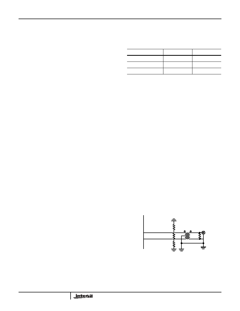
These outputs can be used in a differential-to-single-ended
arrangement to achieve better harmonic rejection. The
SFDR measurements in this data sheet were performed with
a 1:1 transformer on the output of the DAC (see Figure 1).
With the center tap grounded, the output swing of pins 21
and 22 will be biased at zero volts. It is important to note
here that the negative voltage output compliance range limit
is -300mV, imposing a maximum of 600mVP-P amplitude
with this configuration. The loading as shown in Figure 1 will
result in a 500mV signal at the output of the transformer if
the full scale output current of the DAC is set to 20mA.
VOUT = 2 x IOUT x REQ, where REQ is ~12.5
TABLE 1. INPUT CODING vs OUTPUT CURRENT
INPUT CODE (D9-D0)
IOUTA (mA)
IOUTB (mA)
11111 11111
20
0
10000 00000
10
00000 00000
0
20
PIN 21
PIN 22
VOUT = (2 x IOUT x REQ)V
100
HI5760
50
50
50
IOUTB
IOUTA
FIGURE 42.
HI5760
相关PDF资料 |
PDF描述 |
|---|---|
| VI-20F-MY-F4 | CONVERTER MOD DC/DC 72V 50W |
| VI-20F-MY-F3 | CONVERTER MOD DC/DC 72V 50W |
| VE-B1V-MV-F1 | CONVERTER MOD DC/DC 5.8V 75W |
| VI-20F-MY-F1 | CONVERTER MOD DC/DC 72V 50W |
| VI-B1V-MV-F4 | CONVERTER MOD DC/DC 5.8V 75W |
相关代理商/技术参数 |
参数描述 |
|---|---|
| HI5762 | 制造商:INTERSIL 制造商全称:Intersil Corporation 功能描述:Dual 10-Bit, 60MSPS A/D Converter with Internal Voltage Reference |
| HI5762/4IN | 制造商:未知厂家 制造商全称:未知厂家 功能描述:Converter IC |
| HI5762/6IN | 功能描述:CONV A/DDUAL 10BIT 60MSPS 44MQFP RoHS:否 类别:集成电路 (IC) >> 数据采集 - 模数转换器 系列:- 产品培训模块:Lead (SnPb) Finish for COTS Obsolescence Mitigation Program 标准包装:2,500 系列:- 位数:12 采样率(每秒):3M 数据接口:- 转换器数目:- 功率耗散(最大):- 电压电源:- 工作温度:- 安装类型:表面贴装 封装/外壳:SOT-23-6 供应商设备封装:SOT-23-6 包装:带卷 (TR) 输入数目和类型:- |
| HI5762/6INZ | 功能描述:模数转换器 - ADC W/ANNEAL 44L MQFP IN A/D 10B 60MSPS VREF RoHS:否 制造商:Texas Instruments 通道数量:2 结构:Sigma-Delta 转换速率:125 SPs to 8 KSPs 分辨率:24 bit 输入类型:Differential 信噪比:107 dB 接口类型:SPI 工作电源电压:1.7 V to 3.6 V, 2.7 V to 5.25 V 最大工作温度:+ 85 C 安装风格:SMD/SMT 封装 / 箱体:VQFN-32 |
| HI5762_10 | 制造商:INTERSIL 制造商全称:Intersil Corporation 功能描述:Dual 10-Bit, 60MSPS A/D Converter with Internal Voltage Reference |
发布紧急采购,3分钟左右您将得到回复。