- 您现在的位置:买卖IC网 > PDF目录385380 > HI5762EVAL2 (Intersil Corporation) Dual 10-Bit, 60MSPS A/D Converter with Internal Voltage Reference PDF资料下载
参数资料
| 型号: | HI5762EVAL2 |
| 厂商: | Intersil Corporation |
| 英文描述: | Dual 10-Bit, 60MSPS A/D Converter with Internal Voltage Reference |
| 中文描述: | 双10位,60MSPS的A / D转换器内部电压基准 |
| 文件页数: | 11/14页 |
| 文件大小: | 133K |
| 代理商: | HI5762EVAL2 |
27
As illustrated in the functional block diagram and the timing
diagram in Figure 1, eight identical pipeline subconverter
stages, each containing a two-bit flash converter and a two-
bit multiplying digital-to-analog converter, follow the S/H
circuit with the ninth stage being a two bit flash converter.
Each converter stage in the pipeline will be sampling in one
phase and amplifying in the other clock phase. Each
individual subconverter clock signal is offset by 180 degrees
from the previous stage clock signal resulting in alternate
stages in the pipeline performing the same operation.
The output of each of the eight identical two-bit subconverter
stages is a two-bit digital word containing a supplementary bit
to be used by the digital error correction logic. The output of
each subconverter stage is input to a digital delay line which is
controlled by the internal sampling clock. The function of the
digital delay line is to time align the digital outputs of the eight
identical two-bit subconverter stages with the corresponding
output of the ninth stage flash converter before applying the
eighteen bit result to the digital error correction logic. The
digital error correction logic uses the supplementary bits to
correct any error that may exist before generating the final ten
bit digital data output of the converter.
Because of the pipeline nature of this converter, the digital
data representing an analog input sample is output to the
digital data bus following the 6th cycle of the clock after the
analog sample is taken (see the timing diagram in Figure 1).
This time delay is specified as the data latency. After the
data latency time, the digital data representing each
succeeding analog sample is output during the following
clock cycle. The digital output data is provided in offset
binary format (see Table 1, A/D Code Table).
Internal Reference Voltage Output, V
REFOUT
The HI5762 is equipped with an internal reference voltage
generator, therefore, no external reference voltage is
required. V
ROUT
must be connected to V
RIN
when using the
internal reference voltage.
An internal band-gap reference voltage followed by an
amplifier/buffergeneratestheprecision+2.5Vreferencevoltage
used by the converter. A band-gap reference circuit is used to
generate a precision +1.25V internal reference voltage. This
voltage is then amplified by a wide-band uncompensated
operational amplifier connected in a gain-of-two configuration.
An external, user-supplied, 0.1
μ
F capacitor connected from the
V
ROUT
output pin to analog ground is used to set the dominant
pole and to maintain the stability of the operational amplifier.
Reference Voltage Input, V
REFIN
The HI5762 is designed to accept a +2.5V reference voltage
source at the V
RIN
input pin. Typical operation of the
converter requires V
RIN
to be set at +2.5V. The HI5762 is
tested with V
RIN
connected to V
ROUT
yielding a fully
differential analog input voltage range of
±
0.5V.
The user does have the option of supplying an external +2.5V
reference voltage. As a result of the high input impedance
presented at the V
RIN
input pin, 1.25k
typically, the external
reference voltage being used is only required to source 2mA
of reference input current. In the situation where an external
reference voltage will be used an external 0.1
μ
F capacitor
must
be connected from the V
ROUT
output pin to analog
ground in order to maintain the stability of the internal
operational amplifier.
In order to minimize overall converter noise it is
recommended that adequate high frequency decoupling be
provided at the reference voltage input pin, V
RIN
.
Analog Input, Differential Connection
The analog input of the HI5762 is a differential input that can
be configured in various ways depending on the signal
source and the required level of performance. A fully
differential connection (Figure 16 and Figure 17) will deliver
the best performance from the converter.
Since the HI5762 is powered by a single +5V analog supply,
the analog input is limited to be between ground and +5V.
For the differential input connection this implies the analog
input common mode voltage can range from 0.25V to 4.75V.
The performance of the ADC does not change significantly
with the value of the analog input common mode voltage.
A DC voltage source, I/QV
DC
, equal to 3.0V (typical), is
made available to the user to help simplify circuit design
when using an AC coupled differential input. This low output
impedance voltage source is not designed to be a reference
but makes an excellent DC bias source and stays well within
the analog input common mode voltage range over
temperature.
For the AC coupled differential input (Figure 16) and with V
RIN
connected to V
ROUT
, full scale is achieved when the V
IN
and
-V
IN
input signals are 0.5V
P-P
, with -V
IN
being 180 degrees
out of phase with V
IN
. The converter will be at positive full
scale when the I/Q
IN
+ input is at V
DC
+ 0.25V and the I/Q
IN
-
input is at V
DC
- 0.25V (I/Q
IN
+ - I/Q
IN
- = +0.5V). Conversely,
the converter will be at negative full scale when the I/Q
IN
+
input is equal to V
DC
- 0.25V and I/Q
IN
- is at
V
DC
+ 0.25V (I/Q
IN
+ - I/Q
IN
- = -0.5V).
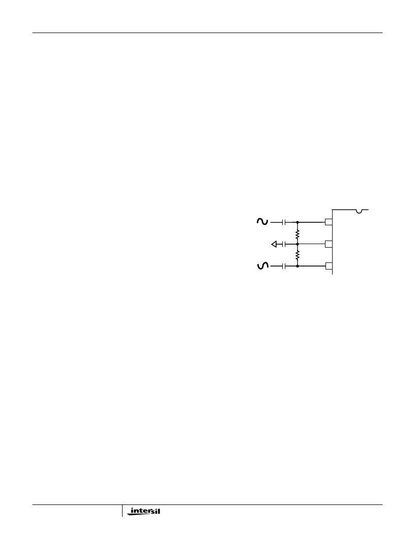
I/Q
IN
+
I/QV
DC
I/Q
IN
-
HI5762
V
IN
-V
IN
R
R
FIGURE 16. AC COUPLED DIFFERENTIAL INPUT
HI5762
相关PDF资料 |
PDF描述 |
|---|---|
| HI5780JCQ | 10-Bit, 80 MSPS, High Speed, Low Power D/A Converter |
| HI5780 | 10-Bit, 80 MSPS, High Speed, Low Power D/A Converter |
| HI5780-EV | 10-Bit, 80 MSPS, High Speed, Low Power D/A Converter |
| HI5800-EV | 12-Bit, 3MSPS, Sampling A/D Converter |
| HI5800JCD | 12-Bit, 3MSPS, Sampling A/D Converter |
相关代理商/技术参数 |
参数描述 |
|---|---|
| HI5766 | 制造商:INTERSIL 制造商全称:Intersil Corporation 功能描述:10-Bit, 60 MSPS A/D Converter |
| HI5766_05 | 制造商:INTERSIL 制造商全称:Intersil Corporation 功能描述:10-Bit, 60MSPS A/D Converter |
| HI5766EVAL1 | 制造商:Rochester Electronics LLC 功能描述:- Bulk 制造商:Harris Corporation 功能描述: |
| HI5766KCA | 功能描述:IC ADC 10-BIT 60MSPS 28-SSOP RoHS:否 类别:集成电路 (IC) >> 数据采集 - 模数转换器 系列:- 产品培训模块:Lead (SnPb) Finish for COTS Obsolescence Mitigation Program 标准包装:2,500 系列:- 位数:12 采样率(每秒):3M 数据接口:- 转换器数目:- 功率耗散(最大):- 电压电源:- 工作温度:- 安装类型:表面贴装 封装/外壳:SOT-23-6 供应商设备封装:SOT-23-6 包装:带卷 (TR) 输入数目和类型:- |
| HI5766KCAZ | 功能描述:模数转换器 - ADC A/D 10-BIT 60MSPS 28 SSOP COM TEMP RoHS:否 制造商:Texas Instruments 通道数量:2 结构:Sigma-Delta 转换速率:125 SPs to 8 KSPs 分辨率:24 bit 输入类型:Differential 信噪比:107 dB 接口类型:SPI 工作电源电压:1.7 V to 3.6 V, 2.7 V to 5.25 V 最大工作温度:+ 85 C 安装风格:SMD/SMT 封装 / 箱体:VQFN-32 |
发布紧急采购,3分钟左右您将得到回复。