- 您现在的位置:买卖IC网 > PDF目录385380 > HI5780JCQ (HARRIS SEMICONDUCTOR) 10-Bit, 80 MSPS, High Speed, Low Power D/A Converter PDF资料下载
参数资料
| 型号: | HI5780JCQ |
| 厂商: | HARRIS SEMICONDUCTOR |
| 元件分类: | DAC |
| 英文描述: | 10-Bit, 80 MSPS, High Speed, Low Power D/A Converter |
| 中文描述: | PARALLEL, WORD INPUT LOADING, 0.006 us SETTLING TIME, 10-BIT DAC, PQFP32 |
| 文件页数: | 7/8页 |
| 文件大小: | 75K |
| 代理商: | HI5780JCQ |
10-1722
HI5780
Detailed Description
The HI5780 is a 10-bit, current out D/A converter. The DAC
can convert at 80 MSPS and runs on +5V supplies. The
HI5780 achieves its low power and high speed performance
from an advanced CMOS process. The HI5780 consumes
150mW (Maximum) and has a power down mode that only
consumes 1.25mW when in sleep mode. The HI5780 is an
excellent converter to be used for communications applica-
tions and high performance video systems.
Digital Inputs
The HI5780 is a TTL/CMOS-compatible D/A. Data is latched
by a 10-bit latch. Once latched data inputs D0 (LSB) thru D9
(MSB) are decoded to the internal current cells; the internal
latch and switching current source controls are implemented
in CMOS technology to maintain high switching speeds and
low power consumption.
Clocks and Termination
The internal 10-bit register is updated on the rising edge of
the clock. Since the HI5780 clock rate can run to 80MHz, to
minimize reflections and clock noise into the part, proper ter-
mination should be used. In PCB layout clock runs should be
kept short and have a minimum of loads. To guarantee con-
sistent results from board to board, controlled impedance
PCBs should be used with a characteristic line impedance,
Z
O
, of 50
.
To terminate the clock line a shunt terminator to ground is the
most effective type at a 80 MSPS clock rate. A typical value
for termination can be determined by the equation:
for the termination resistor. For a controlled impedance
board with a Z
O
of 50
, the R
T
= 50
. Shunt termination is
best used at the receiving end of the transmission line or as
close to the HI5780 CLK pin as possible.
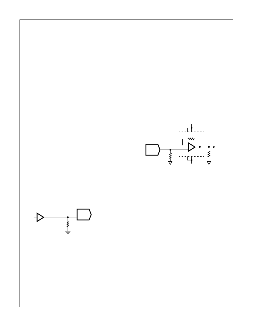
FIGURE 9. AC TERMINATION OF THE HI5780 CLOCK LINE
Rise and Fall times and propagation delay of the line will be
affected by the Shunt Terminator. The terminator can be
connected to DGND.
Noise Reduction
To reduce power supply noise, separate analog and digital
power supplies should be used with 0.1
μ
F and 0.01
μ
F
ceramic capacitors placed as close to the body of the
HI5780 as possible on the analog (AV
DD
) and digital (DV
DD
)
supplies. The analog and digital ground returns should be
connected together back at the device to ensure proper
operation on power up.
R
T
Z
O
,
=
R
T
= 50
HI5780
DAC
CLK
Z
O
= 50
Reference
The internal reference in the HI5780 is a 1.25V (typical)
bandgap voltage reference. The internal reference is buff-
ered by an amplifier to provide adequate drive for the current
cells. Reference Out (REF
OUT
) is connected to the V
REF
pin.
The Full Scale Output Current is controlled by the resistor
connected to I
REF
. The full scale output voltage, is set by the
following equation:
Applications
Voltage Conversion of the Output
To convert the output current of the D/A converter to a
voltage, an amplifier should be used as shown in Figure 5.
The DAC needs a 50
termination resistor on the I
OUT
pin to
ensure proper settling. The HFA1110 has an internal feed-
back resistor to compensate for high frequency operation.
FIGURE 10. HIGH SPEED CURRENT TO VOLTAGE CONVERSION
Definition of Specifications
Integral Linearity Error, INL,
is the measure of the worst
case point that deviates from a best fit straight line of data
values along the transfer curve.
Differential Linearity Error, DNL,
is the measure of the
step size output deviation from code to code. Ideally the step
size should be 1 LSB. A DNL specification of 1 LSB or less
guarantees monotonicity.
Output Voltage Full Scale Settling Time,
is the time
required from the 50% point on the clock input for a full scale
step to settle within an
1
/
2
LSB error band.
Glitch Area, GE,
is the switching transient appearing on the
output during a code transition. It is measured as the area
under the curve and expressed as a Volt-Time specification.
Differential Gain,
A
V
, is the gain error from an ideal sine
wave with a normalized amplitude.
Differential Phase,
Φ
, is the phase error from and ideal
sine wave.
Spurious Free Dynamic Range, SFDR,
is the amplitude
difference from a fundamental to the largest harmonically or
non-harmonically related spur. A sine wave is loaded into the
D/A and the output filtered at
1
/
2
the clock frequency to elim-
inate noise from clocking alias terms.
V
OUT
(Full Scale) = V
REF
x 16 R
LOAD
/R
REF
)
.
HI5780
DAC
21
4
1
+5V
50
8
5
-5.2V
50
HFA1110
2
6
I
OUT
+
-
相关PDF资料 |
PDF描述 |
|---|---|
| HI5780 | 10-Bit, 80 MSPS, High Speed, Low Power D/A Converter |
| HI5780-EV | 10-Bit, 80 MSPS, High Speed, Low Power D/A Converter |
| HI5800-EV | 12-Bit, 3MSPS, Sampling A/D Converter |
| HI5800JCD | 12-Bit, 3MSPS, Sampling A/D Converter |
| HI5800KCD | 12-Bit, 3MSPS, Sampling A/D Converter |
相关代理商/技术参数 |
参数描述 |
|---|---|
| HI5780JCQ-T | 制造商:Rochester Electronics LLC 功能描述:HI5780JCQ IN TAPE & REEL - Bulk |
| HI5800 | 制造商:INTERSIL 制造商全称:Intersil Corporation 功能描述:12-Bit, 3MSPS, Sampling A/D Converter |
| HI5800_00 | 制造商:INTERSIL 制造商全称:Intersil Corporation 功能描述:12-Bit, 3MSPS, Sampling A/D Converter |
| HI5800BID | 制造商:INTERSIL 制造商全称:Intersil Corporation 功能描述:12-Bit, 3MSPS, Sampling A/D Converter |
| HI5800-EV | 制造商:Rochester Electronics LLC 功能描述:- Bulk |
发布紧急采购,3分钟左右您将得到回复。