- 您现在的位置:买卖IC网 > PDF目录385381 > HI5860 (Intersil Corporation) 12-Bit, 130MSPS, High Speed D/A Converter(12位,130MHz,高速D/A转换器) PDF资料下载
参数资料
| 型号: | HI5860 |
| 厂商: | Intersil Corporation |
| 英文描述: | 12-Bit, 130MSPS, High Speed D/A Converter(12位,130MHz,高速D/A转换器) |
| 中文描述: | 12位,130Msps,高速D / A转换(12位,130MHz的,高速的D / A转换器) |
| 文件页数: | 9/10页 |
| 文件大小: | 690K |
| 代理商: | HI5860 |
9
FN4654.6
May 4, 2005
corresponding components should be located over the
digital ground plane and terminated to the digital ground
plane. The same is true for the analog components and the
analog ground plane. Consult Application Note 9853.
Noise Reduction
To minimize power supply noise, 0.1
μ
F capacitors should be
placed as close as possible to the converter’s power supply
pins, AV
DD
and DV
DD
. Also, the layout should be designed
using separate digital and analog ground planes and these
capacitors should be terminated to the digital ground for
DV
DD
and to the analog ground for AV
DD
Additional filtering
of the power supplies on the board is recommended.
Voltage Reference
The internal voltage reference of the device has a nominal
value of +1.2V with a
±
60ppm /
°C
drift coefficient over the full
temperature range of the converter. It is recommended that
a 0.1
μ
F capacitor be placed as close as possible to the
REFIO pin, connected to the analog ground. The REFLO pin
(16) selects the reference. The internal reference can be
selected if pin 16 is tied low (ground). If an external
reference is desired, then pin 16 should be tied high (the
analog supply voltage) and the external reference driven into
REFIO, pin 17. The full scale output current of the converter
is a function of the voltage reference used and the value of
R
SET
I
OUT
should be within the 2mA to 20mA range,
though operation below 2mA is possible, with performance
degradation.
If the internal reference is used, V
FSADJ
will equal
approximately 1.2V (pin 18). If an external reference is used,
V
FSADJ
will equal the external reference. The calculation for
I
OUT
(Full Scale) is:
I
OUT
(Full Scale) = (V
FSADJ
/R
SET)
X 32.
If the full scale output current is set to 20mA by using the
internal voltage reference (1.2V) and a 1.91k
R
SET
resistor, then the input coding to output current will resemble
the following:
Outputs
IOUTA and IOUTB are complementary current outputs. The
sum of the two currents is always equal to the full scale
output current minus one LSB. If single ended use is
desired, a load resistor can be used to convert the output
current to a voltage. It is recommended that the unused
output be either grounded or equally terminated. The voltage
developed at the output must not violate the output voltage
compliance range of -0.3V to 1.25V. R
LOAD
(the impedance
loading each current output) should be chosen so that the
desired output voltage is produced in conjunction with the
output full scale current. If a known line impedance is to be
driven, then the output load resistor should be chosen to
match this impedance. The output voltage equation is:
V
OUT
= I
OUT
X R
LOAD
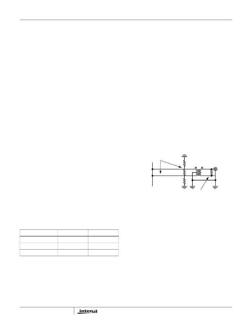
These outputs can be used in a differential-to-single-ended
arrangement to achieve better harmonic rejection. The
SFDR measurements in this data sheet were performed with
a 1:1 transformer on the output of the DAC (see Figure 1).
With the center tap grounded, the output swing of pins 21
and 22 will be biased at zero volts. The loading as shown in
Figure 1 will result in a 500mV signal at the output of the
transformer if the full scale output current of the DAC is set
to 20mA.
V
OUT
= 2 x I
OUT
x R
EQ
, where R
EQ
is ~12.5
. Allowing the
center tap to float will result in identical transformer output,
however the output pins of the DAC will have positive DC
offset. Since the DAC’s output voltage compliance range is -
0.3V to +1.25V, the center tap may need to be left floating or
DC offset in order to increase the amount of signal swing
available. The 50
load on the output of the transformer
represents the spectrum analyzer’s input impedance.
TABLE 1. INPUT CODING vs OUTPUT CURRENT
INPUT CODE (D11-D0)
IOUTA (mA)
IOUTB (mA)
11 11111 11111
20
0
10 00000 00000
10
10
00 00000 00000
0
20
PIN 21
PIN 22
HI5860
100
50
50
50
FIGURE 1.
IOUTB
IOUTA
V
OUT
= (2 x I
OUT
x R
EQ
)V
R
EQ
IS THE IMPEDANCE
LOADING EACH OUTPUT
SPECTRUM ANALYZER
50
REPRESENTS THE
HI5860
相关PDF资料 |
PDF描述 |
|---|---|
| HI5905QML | 14 Bits 5MSPS Military A/D Converter(14位、5MSPS军用ADC) |
| HI5905 | 14-Bit, 5 MSPS A/D Converter |
| HI5905IN | 14-Bit, 5 MSPS A/D Converter |
| HI5905N | 14-Bit, 5 MSPS, Military A/D Converter |
| HI5905EVAL2 | 14-Bit, 5 MSPS A/D Converter |
相关代理商/技术参数 |
参数描述 |
|---|---|
| HI5860 WAF | 制造商:Intersil Corporation 功能描述: |
| HI5860_05 | 制造商:INTERSIL 制造商全称:Intersil Corporation 功能描述:12-Bit, 130MSPS, High Speed D/A Converter |
| HI5860_08 | 制造商:INTERSIL 制造商全称:Intersil Corporation 功能描述:12-Bit, 130MSPS, High Speed D/A Converter |
| HI5860IA | 功能描述:CONV D/A 12BIT 130MSPS 28-TSSOP RoHS:否 类别:集成电路 (IC) >> 数据采集 - 数模转换器 系列:- 标准包装:2,400 系列:- 设置时间:- 位数:18 数据接口:串行 转换器数目:3 电压电源:模拟和数字 功率耗散(最大):- 工作温度:-40°C ~ 85°C 安装类型:表面贴装 封装/外壳:36-TFBGA 供应商设备封装:36-TFBGA 包装:带卷 (TR) 输出数目和类型:* 采样率(每秒):* |
| HI5860IA-T | 功能描述:CONV D/A 12BIT 130MSPS 28-TSSOP RoHS:否 类别:集成电路 (IC) >> 数据采集 - 数模转换器 系列:- 标准包装:2,400 系列:- 设置时间:- 位数:18 数据接口:串行 转换器数目:3 电压电源:模拟和数字 功率耗散(最大):- 工作温度:-40°C ~ 85°C 安装类型:表面贴装 封装/外壳:36-TFBGA 供应商设备封装:36-TFBGA 包装:带卷 (TR) 输出数目和类型:* 采样率(每秒):* |
发布紧急采购,3分钟左右您将得到回复。