- 您现在的位置:买卖IC网 > PDF目录385381 > HI7190IP (INTERSIL CORP) null24-Bit, High Precision, Sigma Delta A/D Converter PDF资料下载
参数资料
| 型号: | HI7190IP |
| 厂商: | INTERSIL CORP |
| 元件分类: | ADC |
| 英文描述: | null24-Bit, High Precision, Sigma Delta A/D Converter |
| 中文描述: | 1-CH 24-BIT DELTA-SIGMA ADC, SERIAL ACCESS, PDIP20 |
| 封装: | PLASTIC, MS-001AD, DIP-20 |
| 文件页数: | 10/24页 |
| 文件大小: | 187K |
| 代理商: | HI7190IP |
1880
Analog Inputs
The analog input on the HI7190 is a fully differential input
with programmable gain capabilities. The input accepts both
unipolar and bipolar input signals and gains range from 1 to
128. The common mode range of this input is from AV
SS
to
AV
DD
provided that the absolute value of the analog input
voltage lies within the power supplies. The input impedance
of the HI7190 is dependent upon the modulator input sam-
pling rate and the sampling rate varies with the selected
PGIA gain. Table 3 below shows the sampling rates and
input impedances for the different gain settings of the
HI7190. Note that this table is valid only for a 10MHz master
clock. If the input clock frequency is changed then the input
impedance will change accordingly. The equation used to
calculate the input impedance is:
where C
in
is the nominal input capacitance (8pF) and f
S
is
the modulator sampling rate.
Bipolar/Unipolar Input Ranges
The input on the HI7190 can accept either unipolar or bipolar
input voltages. Bipolar or unipolar options are chosen by pro-
gramming the B/U bit of the Control Register. Programming
the part for either unipolar or bipolar operation does not
change the input signal conditioning.
The inputs are differential, and as a result are referenced to
the voltage on the V
INLO
input. For example, if V
INLO
is
+1.25V and the HI7190 is configured for unipolar operation
with a gain of 1 and a V
REF
of +2.5V, the input voltage range
on the V
INLO
input is +1.25V to +3.75V. If V
INLO
is +1.25V
and the HI7190 is configured for bipolar mode with gain of 1
and a V
REF
of +2.5V, the analog input range on the V
INHI
input is -1.25V to +3.75V.
Programmable Gain Instrumentation Amplifier
The Programmable Gain Instrumentation Amplifier allows the
user to directly interface low level sensors and bridges directly
to the HI7190. The PGIA has 4 selectable gain options of 1, 2,
4, 8 which are implemented by multiple sampling of the input
signal. Input signals can be gained up further to 16, 32, 64 or
128. These higher gains are implemented in the digital section
of the design to maintain a high signal to noise ratio through
the front end amplifiers. The gain is digitally programmable in
the Control Register via the serial interface. For optimum
PGIA performance the V
CM
pin should be tied to the mid point
of the analog supplies.
Differential Reference Input
The reference inputs of the of the HI7190, V
RHI
and V
RLO
,
provide a differential reference input capability. The nominal
differential voltage (V
REF
= V
RHI
- V
RLO
) is +2.5V and the
common mode voltage cab be anywhere between AV
SS
and
AV
DD
. Larger values of V
REF
can be used without
degradation in performance with the maximum reference
voltage being V
REF
= +5V. Smaller values of V
REF
can also
be used but performance will be degraded since the LSB
size is reduced.
The full scale range of the HI7190 is defined as:
and V
RHI
must always be greater than V
RLO
for proper
operation of the device.
The reference inputs provide a high impedance dynamic
load similar to the analog inputs and the effective input
impedance for the reference inputs can be calculated in the
same manner as it is for the analog input impedance. The
only difference in the calculation is that C
IN
for the reference
inputs is 10.67pF. Therefor, the input impedance range for
the reference inputs is from 149k
in a gain of 8 or higher
mode to 833k
in the gain of 1 mode.
V
CM
Input
The voltage at the V
CM
input is the voltage that the internal
analog circuitry is referenced to and should always be tied to
the midpoint of the AV
DD
and AV
SS
supplies. This point
provides a common mode input voltage for the internal oper-
ational amplifiers and must be driven from a low noise, low
impedance source if it is not tied to analog ground. Failure to
do so will result in degraded HI7190 performance. It is
recommended that V
CM
be tied to analog ground when
operating off of AV
DD
= +5V and AV
SS
= -5V supplies.
V
CM
also determines the headroom at the upper and lower
ends of the power supplies which is limited by the common
mode input range where the internal operational amplifiers
remain in the linear, high gain region of operation. The
HI7190 is designed to have a range of AV
SS
+1.8V < V
CM
<
AV
DD
- 1.8V. Exceeding this range on the V
CM
pin will
compromise the device performance.
Transducer Burn-Out Current Source
The V
INHI
input of the HI7190 contains a 500nA (Typ) current
source which can be turned on/off via the Control Register.
This current source can be used in checking whether a trans-
ducer has burnt-out or become open before attempting to take
measurements on that channel. When the current source is
turned on an additional offset will be created indicating the
presence of a transducer. The current source is controlled by
the BO bit (Bit 4) in the Control Register and is disabled on
power up. See Figure 8 for an applications circuit.
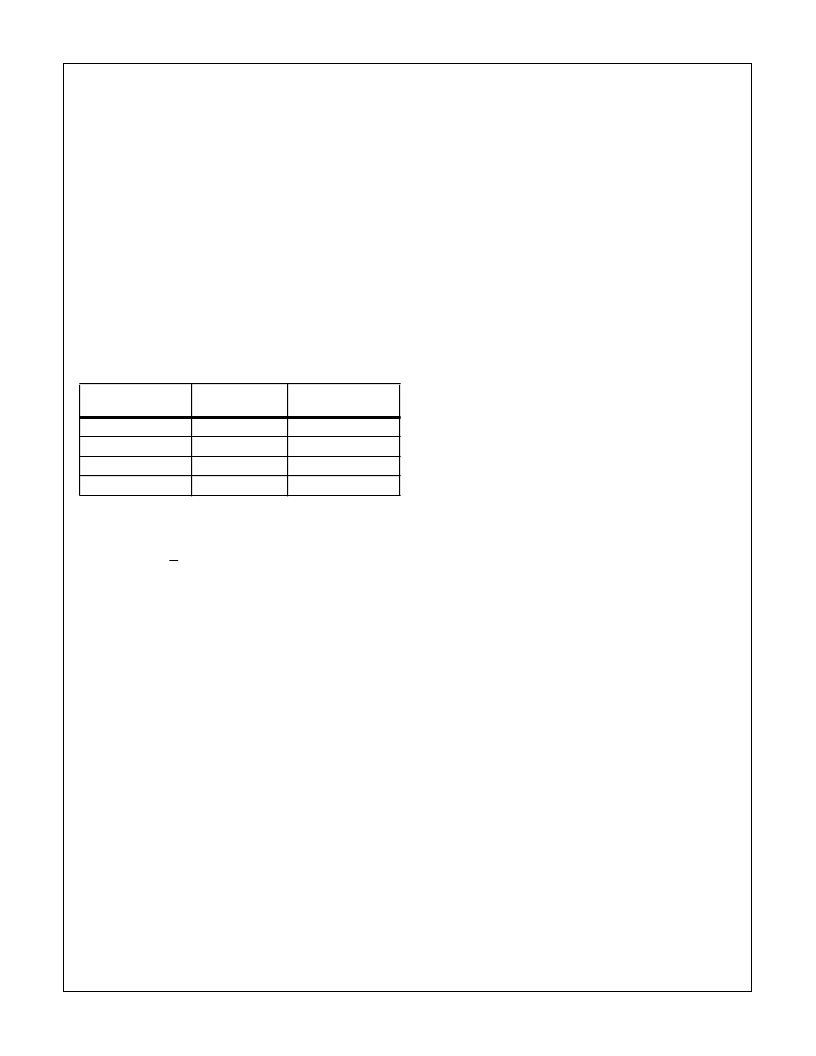
TABLE 3. EFFECTIVE INPUT IMPEDANCE vs GAIN
GAIN
SAMPLING RATE
(kHz)
INPUT IMPEDANCE
(M
)
1
78.125
1.6
2
156.25
0.8
4
312.5
0.4
8, 16, 32, 64, 128
625
0.2
Z
IN
= 1/(C
IN
x f
S
),
FSR
BIPOLAR
= 2 x V
REF
/GAIN
FSR
UNIPOLAR
= V
REF
/GAIN
HI7190
相关PDF资料 |
PDF描述 |
|---|---|
| HI7190EVAL | null24-Bit, High Precision, Sigma Delta A/D Converter |
| HI7190IB | null24-Bit, High Precision, Sigma Delta A/D Converter |
| HIH-3602-A | Humidity Sensor(湿度传感器) |
| HIH-3602-L-CP | Humidity Sensor(湿度传感器) |
| HIN240 | 5V High-Speed RS-232 Transceivers with 0.1uF Capacitors |
相关代理商/技术参数 |
参数描述 |
|---|---|
| HI7190IPZ | 功能描述:模数转换器 - ADC W/ANNEAL ADC 24BIT 1 0HZ SIGMADELTA RoHS:否 制造商:Texas Instruments 通道数量:2 结构:Sigma-Delta 转换速率:125 SPs to 8 KSPs 分辨率:24 bit 输入类型:Differential 信噪比:107 dB 接口类型:SPI 工作电源电压:1.7 V to 3.6 V, 2.7 V to 5.25 V 最大工作温度:+ 85 C 安装风格:SMD/SMT 封装 / 箱体:VQFN-32 |
| HI7191 | 制造商:INTERSIL 制造商全称:Intersil Corporation 功能描述:24-Bit, High Precision, Sigma Delta A/D Converter |
| HI7191_06 | 制造商:INTERSIL 制造商全称:Intersil Corporation 功能描述:24-Bit, High Precision, Sigma Delta A/D Converter |
| HI7191IB | 功能描述:IC ADC 24BIT PROGBL SER 20-SOIC RoHS:否 类别:集成电路 (IC) >> 数据采集 - 模数转换器 系列:- 产品培训模块:Lead (SnPb) Finish for COTS Obsolescence Mitigation Program 标准包装:2,500 系列:- 位数:12 采样率(每秒):3M 数据接口:- 转换器数目:- 功率耗散(最大):- 电压电源:- 工作温度:- 安装类型:表面贴装 封装/外壳:SOT-23-6 供应商设备封装:SOT-23-6 包装:带卷 (TR) 输入数目和类型:- |
| HI7191IBZ | 功能描述:模数转换器 - ADC ADC 24BIT SIGMADELTA 20 IND RoHS:否 制造商:Texas Instruments 通道数量:2 结构:Sigma-Delta 转换速率:125 SPs to 8 KSPs 分辨率:24 bit 输入类型:Differential 信噪比:107 dB 接口类型:SPI 工作电源电压:1.7 V to 3.6 V, 2.7 V to 5.25 V 最大工作温度:+ 85 C 安装风格:SMD/SMT 封装 / 箱体:VQFN-32 |
发布紧急采购,3分钟左右您将得到回复。