参数资料
| 型号: | HI7190IPZ |
| 厂商: | Intersil |
| 文件页数: | 23/25页 |
| 文件大小: | 0K |
| 描述: | IC ADC 24BIT PROGBL SER 20-PDIP |
| 产品培训模块: | Solutions for Industrial Control Applications |
| 标准包装: | 18 |
| 位数: | 24 |
| 数据接口: | 串行,SPI? |
| 转换器数目: | 1 |
| 功率耗散(最大): | 32.5mW |
| 电压电源: | 模拟和数字,双 ± |
| 工作温度: | -40°C ~ 85°C |
| 安装类型: | 通孔 |
| 封装/外壳: | 20-DIP(0.300",7.62mm) |
| 供应商设备封装: | 20-PDIP |
| 包装: | 管件 |
| 输入数目和类型: | 1 个差分,单极;1 个差分,双极 |
7
FN3612.10
June 27, 2006
Pin Descriptions
20 LEAD
DIP, SOIC
PIN NAME
DESCRIPTION
1
SCLK
Serial Interface Clock. Synchronizes serial data transfers. Data is input on the rising edge and output on the
falling edge.
2
SDO
Serial Data OUT. Serial data is read from this line when using a 3-wire serial protocol such as the
Motorola Serial Peripheral Interface.
3
SDIO
Serial Data IN or OUT. This line is bidirectional programmable and interfaces directly to the Intel Standard Serial
Interface using a 2-wire serial protocol.
4CS
Chip Select Input. Used to select the HI7190 for a serial data transfer cycle. This line can be tied to DGND.
5
DRDY
An Active Low Interrupt indicating that a new data word is available for reading.
6
DGND
Digital Supply Ground.
7AVSS
Negative Analog Power Supply (-5V).
8VRLO
External Reference Input. Should be negative referenced to VRHI.
9VRHI
External Reference Input. Should be positive referenced to VRLO.
10
VCM
Common Mode Input. Should be set to halfway between AVDD and AVSS.
11
VINLO
Analog Input LO. Negative input of the PGIA.
12
VINHI
Analog Input HI. Positive input of the PGIA. The VINHI input is connected to a current source that can be used to check
the condition of an external transducer. This current source is controlled via the Control Register.
13
AVDD
Positive Analog Power Supply (+5V).
14
AGND
Analog Supply Ground.
15
DVDD
Positive Digital Supply (+5V).
16
OSC2
Used to connect a crystal source between OSC1 and OSC2. Leave open otherwise.
17
OSC1
Oscillator Clock Input for the device. A crystal connected between OSC1 and OSC2 will provide a clock to the device,
or an external oscillator can drive OSC1. The oscillator frequency should be 10MHz (Typ).
18
RESET
Active Low Reset Pin. Used to initialize the HI7190 registers, filter and state machines.
19
SYNC
Active Low Sync Input. Used to control the synchronization of a number of HI7190s. A logic ‘0’ initializes the converter.
20
MODE
Mode Pin. Used to select between Synchronous Self Clocking (Mode = 1) or Synchronous External Clocking
(Mode = 0) for the Serial Port.
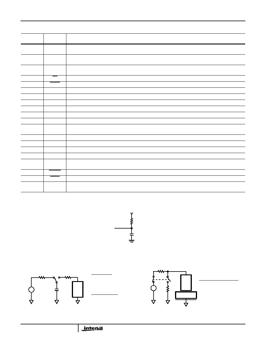
Load Test Circuit
FIGURE 4.
V1
R1
CL (INCLUDES STRAY
DUT
CAPACITANCE)
ESD Test Circuits
FIGURE 5A.
FIGURE 5B.
DUT
HUMAN BODY
CESD = 100pF
MACHINE MODEL
CESD = 200pF
R1
CESD
R1 = 10MΩ
R2
R2 = 1.5kΩ
R2 = 0Ω
±
V
CHARGED DEVICE MODEL
R1
R1 = 1GΩ
R2
R2 = 1Ω
±
V
DUT
DIELECTRIC
HI7190
相关PDF资料 |
PDF描述 |
|---|---|
| V24B48M250BF | CONVERTER MOD DC/DC 48V 250W |
| MS27466E15A5S | CONN RCPT 5POS WALL MT W/SCKT |
| V24B12M250BF3 | CONVERTER MOD DC/DC 12V 250W |
| IDT72V255LA10PF | IC FIFO SS 8192X18 10NS 64-TQFP |
| MS27497T10B99SA | CONN RCPT 7POS WALL MNT W/SCKT |
相关代理商/技术参数 |
参数描述 |
|---|---|
| HI7191 | 制造商:INTERSIL 制造商全称:Intersil Corporation 功能描述:24-Bit, High Precision, Sigma Delta A/D Converter |
| HI7191_06 | 制造商:INTERSIL 制造商全称:Intersil Corporation 功能描述:24-Bit, High Precision, Sigma Delta A/D Converter |
| HI7191IB | 功能描述:IC ADC 24BIT PROGBL SER 20-SOIC RoHS:否 类别:集成电路 (IC) >> 数据采集 - 模数转换器 系列:- 产品培训模块:Lead (SnPb) Finish for COTS Obsolescence Mitigation Program 标准包装:2,500 系列:- 位数:12 采样率(每秒):3M 数据接口:- 转换器数目:- 功率耗散(最大):- 电压电源:- 工作温度:- 安装类型:表面贴装 封装/外壳:SOT-23-6 供应商设备封装:SOT-23-6 包装:带卷 (TR) 输入数目和类型:- |
| HI7191IBZ | 功能描述:模数转换器 - ADC ADC 24BIT SIGMADELTA 20 IND RoHS:否 制造商:Texas Instruments 通道数量:2 结构:Sigma-Delta 转换速率:125 SPs to 8 KSPs 分辨率:24 bit 输入类型:Differential 信噪比:107 dB 接口类型:SPI 工作电源电压:1.7 V to 3.6 V, 2.7 V to 5.25 V 最大工作温度:+ 85 C 安装风格:SMD/SMT 封装 / 箱体:VQFN-32 |
| HI7191IBZ-T | 功能描述:模数转换器 - ADC ADC 24BIT SIGMADELTA 20 IND RoHS:否 制造商:Texas Instruments 通道数量:2 结构:Sigma-Delta 转换速率:125 SPs to 8 KSPs 分辨率:24 bit 输入类型:Differential 信噪比:107 dB 接口类型:SPI 工作电源电压:1.7 V to 3.6 V, 2.7 V to 5.25 V 最大工作温度:+ 85 C 安装风格:SMD/SMT 封装 / 箱体:VQFN-32 |
发布紧急采购,3分钟左右您将得到回复。