- 您现在的位置:买卖IC网 > PDF目录299176 > HIP0045AB (HARRIS SEMICONDUCTOR) 1.75 A 8 CHANNEL, LATCH BASED PRPHL DRVR, PDSO20 PDF资料下载
参数资料
| 型号: | HIP0045AB |
| 厂商: | HARRIS SEMICONDUCTOR |
| 元件分类: | Peripheral Driver |
| 英文描述: | 1.75 A 8 CHANNEL, LATCH BASED PRPHL DRVR, PDSO20 |
| 封装: | PLASTIC, DSO-20 |
| 文件页数: | 6/9页 |
| 文件大小: | 87K |
| 代理商: | HIP0045AB |
6
Signal Pin Descriptions
Power Output Drivers, OUT0 - OUT7 - The input and
output bits corresponding to Output 0 thru Output 7 are
transmitted and received most signicant bit (MSB) rst via
the SPI bus. Outputs OUT0 - 5 are provided with over-
current shutdown. Current Limiting and Thermal Shutdown
are provided on OUT6, 7 for application use as Lamp
Drivers. After a fault shutdown, the control lines remain
active. The fault latches must be cleared by turning the
output off and on to reset the output to an ON state. OUT1, 2
latches may be cleared by the RESET pin.
RESET - Active low reset input. An internal pull-up is
provided on-chip. When this input line is low, all output
drivers are turned-off and the OUT1, 2 fault latches are
cleared. An internal low voltage reset is ORed with the
RESET input. When VCC is less than VLCC_RST, the
internal reset is active.
CE - Active low chip enable. The falling edge of CE loads the
shift register with the output status bits. Data is transferred
from the shift register to the outputs on the rising edge of CE.
The output driver for the MISO pin is enabled when CE goes
low. CE must be a logic low prior to the first serial clock (SCK)
and must remain low until after the last (eighth) serial clock
cycle. All eight MOSI bits of input data must be loaded in the
same sequence of SCK clock input. A digital lter is used in
the CE line to insure that 8 (or a multiple of 8) clock cycles
occurs while CE is active low. After SCK is low for a short
period, tLAG; CE may be changed from low to high to latch the
input data. A low level on CE also activates an internal disable
circuit used for unlatching output states that are in a fault
mode as sensed by an out of saturation condition. A high on
CE forces MISO to a high impedance state. Also, when CE is
high, the octal driver ignores the SCK and MOSI signals.
IN0, 1 - IN0 and IN1 are Channels 0 and 1 direct parallel
input controls. Refer to ‘Special Input Conditions for Channel
0, 1‘ in the following text.
SCK, MISO, MOSI - Refer to the ‘Serial Peripheral Interface’
(SPI) section in the following text.
Serial Peripheral Interface (SPI)
The Serial Peripheral Interface (SPI) is a serial synchronous
bus for control and data transfers. The Clock (SCK), which is
generated by the microcomputer, is active only during data
transfers. In systems using CDP68HC05 family
microcomputers, the inactive clock polarity is determined by
the CPOL bit in the microcomputer’s control register. The
CPOL bit is used in conjunction with the clock phase bit,
CPHA to produce the desired clock data relationship
between the microcomputer and octal driver. The CPHA bit
in general selects the clock edge which captures data and
allows it to change states. For the HIP0045, the CPOL bit
must be set to a logic zero and the CPHA bit to a logic one.
Congured in this manner, MISO (output) data will appear
with every rising edge of the SCK clock pulse, and MOSI
(input) data will be latched into the shift register with every
falling edge of the SCK clock pulse. Also, the steady state
value of the inactive serial clock, SCK, will be at a low level.
Timing diagrams for the serial peripheral interface are shown
in Figure 1.
SPI Signal Descriptions
MOSI (Master Out/Slave In) - Serial data input. Data bytes
are shifted in at this pin, most signicant bit (MSB) rst. The
data is passed directly to the shift register which in turn
controls the latches and output drivers.
MISO (Master In/Slave Out) - Serial data output. Data bytes
are shifted out at this pin, most signicant bit (MSB) rst.
This pin is the serial output from the shift register and is
three stated when CE is high. Diagnostic Failure Register
information is given in Tables 6 and 7. Determination of the
fault condition may be done as a software sequence, based
on MOSI data latched into the shift register and subsequent
data clocked out of the MISO pin.
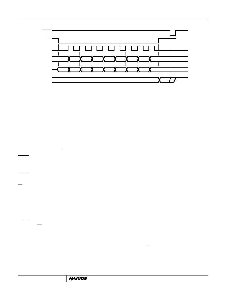
FIGURE 2. BYTE TIMING DIAGRAM WITH ASYNCHRONOUS RESET
Timing Diagrams (Continued)
OLD
NEW
FAULTS
RESET
76543210
RESET
CE
SCK
MOSI
MISO
OUTPUTS
HIP0045
相关PDF资料 |
PDF描述 |
|---|---|
| HIP0050IB | 0.3 A BUF OR INV BASED PRPHL DRVR, PDSO24 |
| HIP1030AS | 1.6 A BUF OR INV BASED PRPHL DRVR, PSFM5 |
| HK10051N2S | 1 ELEMENT, 0.0012 uH, FERRITE-CORE, GENERAL PURPOSE INDUCTOR, SMD |
| HK1005R10K | 1 ELEMENT, 0.1 uH, FERRITE-CORE, GENERAL PURPOSE INDUCTOR, SMD |
| HK100582NK | 1 ELEMENT, 0.082 uH, FERRITE-CORE, GENERAL PURPOSE INDUCTOR, SMD |
相关代理商/技术参数 |
参数描述 |
|---|---|
| HIP0045ABT | 制造商:Rochester Electronics LLC 功能描述:- Tape and Reel |
| HIP0050 | 制造商:INTERSIL 制造商全称:Intersil Corporation 功能描述:0.3A/50V Octal Low Side Power Driver with Serial Bus Control and Over-Current Fault Flag |
| HIP0050IB | 制造商:Rochester Electronics LLC 功能描述:- Bulk |
| HIP0050IB96 | 制造商:Rochester Electronics LLC 功能描述:- Bulk |
| HIP0050IB96S2300 | 制造商:Rochester Electronics LLC 功能描述:- Bulk |
发布紧急采购,3分钟左右您将得到回复。