- 您现在的位置:买卖IC网 > PDF目录299176 > HIP0045AB (HARRIS SEMICONDUCTOR) 1.75 A 8 CHANNEL, LATCH BASED PRPHL DRVR, PDSO20 PDF资料下载
参数资料
| 型号: | HIP0045AB |
| 厂商: | HARRIS SEMICONDUCTOR |
| 元件分类: | Peripheral Driver |
| 英文描述: | 1.75 A 8 CHANNEL, LATCH BASED PRPHL DRVR, PDSO20 |
| 封装: | PLASTIC, DSO-20 |
| 文件页数: | 7/9页 |
| 文件大小: | 87K |
| 代理商: | HIP0045AB |
7
SCK - Serial clock input. The SCK signal clocks the shift
register and new MOSI (input) data will be latched into the
shift register on every falling edge of SCK. The SCK phase
bit, CPHA=1 and the polarity bit, CPOL=0, must be set in the
microcomputer’s control register.
Functional Descriptions
The HIP0045 is a low quiescent power, high voltage, high
current, octal, serial low side driver featuring eight channels
of open drain MOS output drivers. Referring to the Detailed
Block Diagram, the drivers have low rDSON and low
saturation voltage with over-voltage drain-to-gate zener
clamp circuits. Each output is short circuit protected and
suited for driving resistive or inductive loads such as
solenoids, relays and lamps. Data is transmitted to the
device serially using the Serial Peripheral Interface (SPI)
protocol. Each channel is independently controlled by an
output latch and a common RESET line that disables all
eight outputs. Byte timing with asynchronous reset is shown
in Figure 2.
The circuit receives 8-bit serial data by means of the serial input
(MOSI), and stores this data in an internal register to control the
output drivers. The serial output (MISO) provides 8-bit
diagnostic data representing the voltage level at the driver
output. This allows the microcomputer to diagnose the
condition at the output drivers. The device is selected when the
chip enable (CE) line is low. When (CE) is high, the device is
deselected and the serial output (MISO) is placed in a three-
state high impedance mode. The device shifts serial data on
the rising edge of the serial clock (SCK), and latches data on
the falling edge. On the rising edge of chip enable (CE), new
input data from the shift register is latched to control the output
drivers. The falling edge of chip enable (CE) transfers the
output drivers fault information back to the shift register. The
output drivers have low ON voltage at rated current, and are
monitored by a comparator for an out of saturation condition, in
which case the output driver with the fault becomes unlatched
and diagnostic data is sent to the microcomputer via the MISO
line. A typical microcomputer interface circuit is shown in
Figure 3.
SPI Shift Register
The SPI shift register has both serial and parallel inputs and
outputs. Serial output and input data are simultaneously
transferred to and from the SPI bus. The serial input data is
parallel latched into the 8-Bit Output Latch of the HIP0045 at
the end of a data transfer. Diagnostic data, Diag0-7 is
transferred to the shift register when CE goes low at the
beginning of a data transfer cycle.
8-Bit Output Latch
The 8-Bit Output Latch is used to control the output drivers.
New serial data is transferred from the shift register to the
8-Bit Output Latch when CE goes high. The 8-Bit Output
Latch is cleared by an active low RESET signal.
Output Drivers
The output drivers provide an active low output of 500mA
nominal with current limiting set to greater than 1.05A to
allow for high inrush currents. In addition, each output is
provided with a voltage drain-to-gate clamp circuit to limit
inductive transients. Each output driver is also monitored by
a comparator for an out of saturation condition. If the output
voltage of an ON output pin exceeds the saturation voltage
limit, a fault latch turns off the output. The threshold
comparators are used to detect shorts to the power supply,
shorts to ground and open loads. Each comparator provides
status data to the shift register for diagnostic feedback. An
internal pull-down current, ISK at each output will provide an
indicator for low output voltage if the output is programmed
OFF and the output line is open. Refer to Tables 6 and 7 for
Fault information versus output control and VREF. Note that
VREF is the out-of-saturation threshold for an ON state.
When the output is switched off and VREF is low, an open-
load or ground fault is indicated.
CE High to Low Transition
When CE is low the three-state MISO pin is enabled. On the
falling edge of CE, diagnostic and status data from the
output voltage comparators will be latched into the shift
register. During the time that CE is low, data bytes controlling
the output drivers are shifted in at the MOSI pin most
signicant bit (MSB) rst. Tables 1, 2 and 3 dene the logic
state for control of each output and Table 4 denes the
control bit structure.
CE Low to High Transition
When the last serial data bit has been shifted into the MOSI
pin, CE pin is pulled high to transfer data from the shift register
into the 8-bit parallel output latch to activate the outputs. The
serial clock input pin (SCK) should be low during CE
transitions to avoid false clocking of the shift register. The SCK
input is gated by CE so that the SCK input is ignored when CE
is high.
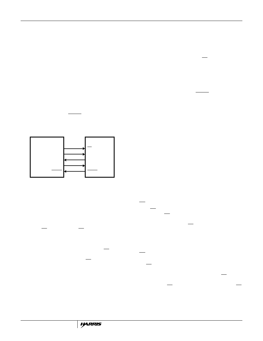
PORT
MOSI
MISO
SCK
RESET
CE
MOSI
MISO
SCK
RESET
CDP68HC05C4
MICROCOMPUTER
HIP0045
FIGURE 3. TYPICAL MICROCOMPUTER INTERFACE WITH
THE HIP0045
HIP0045
相关PDF资料 |
PDF描述 |
|---|---|
| HIP0050IB | 0.3 A BUF OR INV BASED PRPHL DRVR, PDSO24 |
| HIP1030AS | 1.6 A BUF OR INV BASED PRPHL DRVR, PSFM5 |
| HK10051N2S | 1 ELEMENT, 0.0012 uH, FERRITE-CORE, GENERAL PURPOSE INDUCTOR, SMD |
| HK1005R10K | 1 ELEMENT, 0.1 uH, FERRITE-CORE, GENERAL PURPOSE INDUCTOR, SMD |
| HK100582NK | 1 ELEMENT, 0.082 uH, FERRITE-CORE, GENERAL PURPOSE INDUCTOR, SMD |
相关代理商/技术参数 |
参数描述 |
|---|---|
| HIP0045ABT | 制造商:Rochester Electronics LLC 功能描述:- Tape and Reel |
| HIP0050 | 制造商:INTERSIL 制造商全称:Intersil Corporation 功能描述:0.3A/50V Octal Low Side Power Driver with Serial Bus Control and Over-Current Fault Flag |
| HIP0050IB | 制造商:Rochester Electronics LLC 功能描述:- Bulk |
| HIP0050IB96 | 制造商:Rochester Electronics LLC 功能描述:- Bulk |
| HIP0050IB96S2300 | 制造商:Rochester Electronics LLC 功能描述:- Bulk |
发布紧急采购,3分钟左右您将得到回复。