- 您现在的位置:买卖IC网 > PDF目录385382 > HIP6004E (Intersil Corporation) Buck and Synchronous-Rectifier (PWM) Controller and Output Voltage Monitor PDF资料下载
参数资料
| 型号: | HIP6004E |
| 厂商: | Intersil Corporation |
| 英文描述: | Buck and Synchronous-Rectifier (PWM) Controller and Output Voltage Monitor |
| 中文描述: | 巴克和同步整流(PWM)控制器和输出电压监视器 |
| 文件页数: | 6/12页 |
| 文件大小: | 317K |
| 代理商: | HIP6004E |
6
sink develops a voltage across R
OCSET
that is referenced to
V
IN
. When the voltage across the upper MOSFET (also
referenced to V
IN
) exceeds the voltage across R
OCSET
, the
overcurrent function initiates a soft-start sequence. The soft-
start function discharges C
SS
with a 10
μ
A current sink and
inhibits PWM operation. The soft-start function recharges
C
SS
, and PWM operation resumes with the error amplifier
clamped to the SS voltage. Should an overload occur while
recharging C
SS
, the soft-start function inhibits PWM operation
while fully charging C
SS
to 4V to complete its cycle. Figure 4
shows this operation with an overload condition. Note that the
inductor current increases to over 15A during the C
SS
charging interval and causes an overcurrent trip. The
converter dissipates very little power with this method. The
measured input power for the conditions of Figure 4 is 2.5W.
The overcurrent function will trip at a peak inductor current
(I
PEAK)
determined by:
where I
OCSET
is the internal OCSET current source (200
μ
A
typical). The OC trip point varies mainly due to the
MOSFET’s r
DS(ON)
variations. To avoid overcurrent tripping
in the normal operating load range, find the R
OCSET
resistor
from the equation above with:
1. The maximum r
DS(ON)
at the highest junction temperature.
2. The minimum I
OCSET
from the specification table.
3. Determine I
PEAK
for
where
I is the output inductor ripple current.
,
For an equation for the ripple current see the section under
component guidelines titled “Output Inductor Selection”.
A small, ceramic capacitor should be placed in parallel with
R
OCSET
to smooth the voltage across R
OCSET
in the
presence of switching noise on the input voltage.
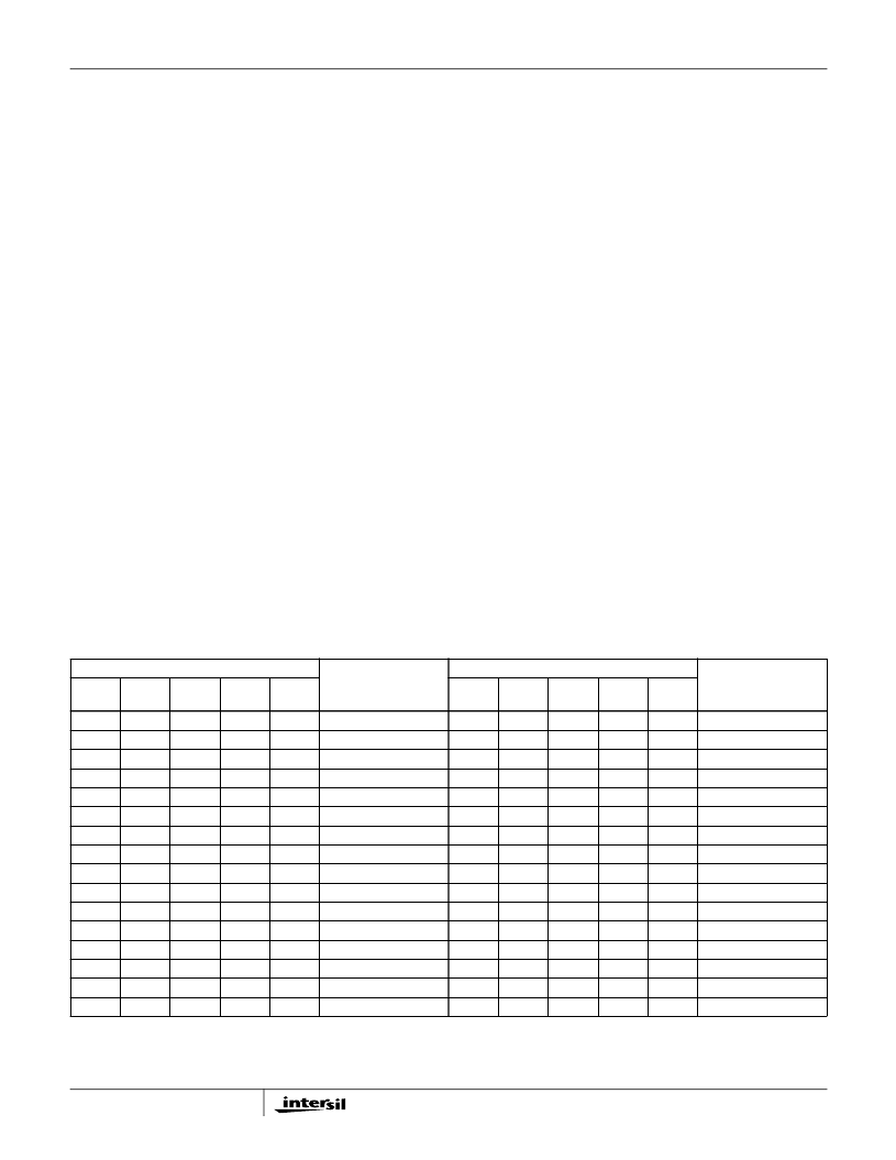
Output Voltage Program
The output voltage of a HIP6004E converter is programmed
to discreet levels between 1.05V
DC
and 1.825V
DC
. The
voltage identification (VID) pins program an internal voltage
reference (DACOUT) with a TTL-compatible 5-bit digital-to-
analog converter (DAC). The level of DACOUT also sets the
PGOOD and OVP thresholds. Table 1 specifies the DACOUT
voltage for the 32 different combinations of connections on the
VID pins. The output voltage should not be adjusted while the
converter is delivering power. Remove input power before
changing the output voltage. Adjusting the output voltage
during operation could toggle the PGOOD signal and exercise
the overvoltage protection.
Application Guidelines
Layout Considerations
As in any high frequency switching converter, layout is very
important. Switching current from one power device to another
can generate voltage transients across the impedances of the
interconnecting bond wires and circuit traces. These
interconnecting impedances should be minimized by using
wide, short-printed circuit traces. The critical components
should be located as close together as possible, using ground
plane construction or single point grounding.
I
PEAK
I
x R
DS ON
)
----------------------------------------------------
=
I
PEAK
I
OUT MAX
(
)
I
(
)
2
+
>
TABLE 1. OUTPUT VOLTAGE PROGRAM
PIN NAME
NOMINAL OUTPUT
VOLTAGE DACOUT
1.050
1.075
1.100
1.125
1.150
1.175
1.200
1.225
1.250
1.275
1.300
1.325
1.350
1.375
1.400
1.425
PIN NAME
NOMINAL OUTPUT
VOLTAGE DACOUT
1.450
1.475
1.500
1.525
1.550
1.575
1.600
1.625
1.650
1.675
1.700
1.725
1.750
1.775
1.800
1.825
VID25
mV
0
1
0
1
0
1
0
1
0
1
0
1
0
1
0
1
NOTE: 0 = connected to GND or V
SS
, 1 = connected to V
DD
through pull-up resistors or leave the pins floating. Internal pull-ups will force the floating
VID pins to HIGH.
VID3
0
0
0
0
0
0
0
0
0
0
1
1
1
1
1
1
VID2
1
1
0
0
0
0
0
0
0
0
1
1
1
1
1
1
VID1
0
0
1
1
1
1
0
0
0
0
1
1
1
1
0
0
VID0
0
0
1
1
0
0
1
1
0
0
1
1
0
0
1
1
VID25
mV
0
1
0
1
0
1
0
1
0
1
0
1
0
1
0
1
VID3
1
1
1
1
1
1
1
1
1
1
0
0
0
0
0
0
VID2
1
1
0
0
0
0
0
0
0
0
1
1
1
1
1
1
VID1
0
0
1
1
1
1
0
0
0
0
1
1
1
1
0
0
VID0
0
0
1
1
0
0
1
1
0
0
1
1
0
0
1
1
HIP6004E
相关PDF资料 |
PDF描述 |
|---|---|
| HIP6004ECB | Buck and Synchronous-Rectifier (PWM) Controller and Output Voltage Monitor |
| HIP6004ECV | Buck and Synchronous-Rectifier (PWM) Controller and Output Voltage Monitor |
| HIP6013 | FPGA - 100000 SYSTEM GATE 2.5 VOLT - NOT RECOMMENDED for NEW DESIGN |
| HIP6013CB | FPGA - 100000 SYSTEM GATE 2.5 VOLT - NOT RECOMMENDED for NEW DESIGN |
| HIP6014 | Buck and Synchronous-Rectifier (PWM) Controller and Output Voltage Monitor |
相关代理商/技术参数 |
参数描述 |
|---|---|
| HIP6004ECB | 功能描述:IC CTRLR PWM VOLTAGE MON 20-SOIC RoHS:否 类别:集成电路 (IC) >> PMIC - 稳压器 - 专用型 系列:- 产品培训模块:Lead (SnPb) Finish for COTS Obsolescence Mitigation Program 标准包装:2,000 系列:- 应用:电源,ICERA E400,E450 输入电压:4.1 V ~ 5.5 V 输出数:10 输出电压:可编程 工作温度:-40°C ~ 85°C 安装类型:表面贴装 封装/外壳:42-WFBGA,WLCSP 供应商设备封装:42-WLP 包装:带卷 (TR) |
| HIP6004ECB-T | 功能描述:IC CTRLR PWM VOLTAGE MON 20-SOIC RoHS:否 类别:集成电路 (IC) >> PMIC - 稳压器 - 专用型 系列:- 产品培训模块:Lead (SnPb) Finish for COTS Obsolescence Mitigation Program 标准包装:2,000 系列:- 应用:电源,ICERA E400,E450 输入电压:4.1 V ~ 5.5 V 输出数:10 输出电压:可编程 工作温度:-40°C ~ 85°C 安装类型:表面贴装 封装/外壳:42-WFBGA,WLCSP 供应商设备封装:42-WLP 包装:带卷 (TR) |
| HIP6004ECBZ | 功能描述:电压模式 PWM 控制器 BUCK & SYNCHCTPWMCNTRLR RoHS:否 制造商:Texas Instruments 输出端数量:1 拓扑结构:Buck 输出电压:34 V 输出电流: 开关频率: 工作电源电压:4.5 V to 5.5 V 电源电流:600 uA 最大工作温度:+ 125 C 最小工作温度:- 40 C 封装 / 箱体:WSON-8 封装:Reel |
| HIP6004ECBZ-T | 功能描述:电压模式 PWM 控制器 BUCK & SYNCH -RECT PWMCNTRLR & OUTPUT RoHS:否 制造商:Texas Instruments 输出端数量:1 拓扑结构:Buck 输出电压:34 V 输出电流: 开关频率: 工作电源电压:4.5 V to 5.5 V 电源电流:600 uA 最大工作温度:+ 125 C 最小工作温度:- 40 C 封装 / 箱体:WSON-8 封装:Reel |
| HIP6004ECV | 功能描述:IC CTRLR PWM VOLTAGE MON 20TSSOP RoHS:否 类别:集成电路 (IC) >> PMIC - 稳压器 - 专用型 系列:- 产品培训模块:Lead (SnPb) Finish for COTS Obsolescence Mitigation Program 标准包装:2,000 系列:- 应用:电源,ICERA E400,E450 输入电压:4.1 V ~ 5.5 V 输出数:10 输出电压:可编程 工作温度:-40°C ~ 85°C 安装类型:表面贴装 封装/外壳:42-WFBGA,WLCSP 供应商设备封装:42-WLP 包装:带卷 (TR) |
发布紧急采购,3分钟左右您将得到回复。