- 您现在的位置:买卖IC网 > PDF目录385382 > HIP6004E (Intersil Corporation) Buck and Synchronous-Rectifier (PWM) Controller and Output Voltage Monitor PDF资料下载
参数资料
| 型号: | HIP6004E |
| 厂商: | Intersil Corporation |
| 英文描述: | Buck and Synchronous-Rectifier (PWM) Controller and Output Voltage Monitor |
| 中文描述: | 巴克和同步整流(PWM)控制器和输出电压监视器 |
| 文件页数: | 9/12页 |
| 文件大小: | 317K |
| 代理商: | HIP6004E |
9
where: I
TRAN
is the transient load current step, t
RISE
is the
response time to the application of load, and t
FALL
is the
response time to the removal of load. With a +5V input
source, the worst-case response time can be either at the
application or removal of load and dependent upon the
DACOUT setting. Be sure to check both of these equations
at the minimum and maximum output levels for the worst
case response time. With a +12V input, and output voltage
level equal to DACOUT, t
FALL
is the longest response time.
Input Capacitor Selection
Use a mix of input bypass capacitors to control the voltage
overshoot across the MOSFETs. Use small ceramic
capacitors for high-frequency decoupling and bulk capacitors
to supply the current needed each time Q
1
turns on. Place the
small ceramic capacitors physically close to the MOSFETs
and between the drain of Q
1
and the source of Q
2
.
The important parameters for the bulk input capacitor are the
voltage rating and the RMS current rating. For reliable
operation, select the bulk capacitor with voltage and current
ratings above the maximum input voltage and largest RMS
current required by the circuit. The capacitor voltage rating
should be at least 1.25 times greater than the maximum
input voltage and a voltage rating of 1.5 times is a
conservative guideline. The RMS current rating requirement
for the input capacitor of a buck regulator is approximately
1/2 the DC load current.
For a through-hole design, several electrolytic capacitors may
be needed. For surface mount designs, solid tantalum
capacitors can be used, but caution must be exercised with
regard to the capacitor surge current rating. These capacitors
must be capable of handling the surge current at power-up.
Some capacitor series available from reputable manufacturers
are surge current tested.
MOSFET Selection/Considerations
The HIP6004E requires 2 N-Channel power MOSFETs. These
should be selected based upon r
DS(ON)
, gate supply
requirements, and thermal management requirements.
In high-current applications, the MOSFET power dissipation,
package selection and heatsink are the dominant design
factors. The power dissipation includes two loss components;
conduction loss and switching loss. The conduction losses are
the largest component of power dissipation for both the upper
and the lower MOSFETs. These losses are distributed between
the two MOSFETs according to duty factor (see the equations
below). Only the upper MOSFET has switching losses, since
the Schottky rectifier clamps the switching node before the
synchronous rectifier turns on. These equations assume linear
voltage current transitions and do not adequately model power
loss due the reverse recovery of the lower MOSFET’s body
diode. The gate-charge losses are dissipated by the HIP6004E
and don't heat the MOSFETs. However, large gate charge
increases the switching interval, t
SW
which increases the upper
MOSFET switching losses. Ensure that both MOSFETs are
within their maximum junction temperature at high ambient
temperature by calculating the temperature rise according to
package thermal-resistance specifications. A separate heatsink
may be necessary depending upon MOSFET power, package
type, ambient temperature and air flow.
Standard-gate MOSFETs are normally recommended for
use with the HIP6004E. However, logic-level gate MOSFETs
can be used under special circumstances. The input voltage,
upper gate drive level, and the MOSFET’s absolute gate-to-
source voltage rating determine whether logic-level
MOSFETs are appropriate.
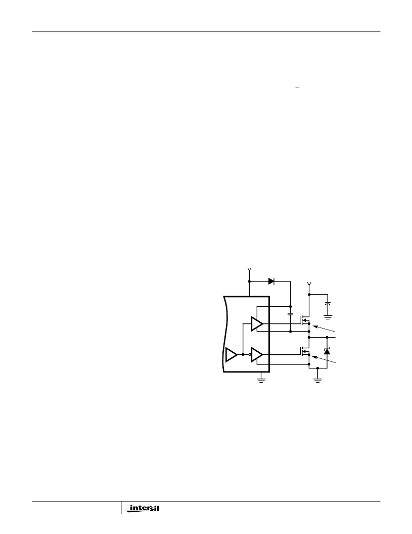
Figure 9 shows the upper gate drive (BOOT pin) supplied by a
bootstrap circuit from V
CC
. The boot capacitor, C
BOOT
develops a floating supply voltage referenced to the PHASE
pin. This supply is refreshed each cycle to a voltage of V
CC
less the boot diode drop (V
D
) when the lower MOSFET, Q
2
turns on. Logic-level MOSFETs can only be used if the
MOSFET’s absolute gate-to-source voltage rating exceeds
the maximum voltage applied to VCC.
Figure 10 shows the upper gate drive supplied by a direct
connection to V
CC
. This option should only be used in
converter systems where the main input voltage is +5V
DC
or
less. The peak upper gate-to-source voltage is approximately
V
CC
less the input supply. For +5V main power and +12V
DC
for the bias, the gate-to-source voltage of Q
1
is 7V. A logic-
level MOSFET is a good choice for Q
1
and a logic-level
MOSFET can be used for Q
2
if its absolute gate-to-source
voltage rating exceeds the maximum voltage applied to V
CC
.
P
UPPER
= Io
2
x r
DS(ON)
x D +1
2
Io x V
IN
x t
SW
x F
S
P
LOWER
= Io
2
x r
DS(ON)
x (1 - D)
Where: D is the duty cycle = V
OUT
/ V
IN
,
t
SW
is the switch ON time, and
F
S
is the switching frequency.
+12V
PGND
HIP6004E
GND
LGATE
UGATE
PHASE
BOOT
VCC
+5V OR +12V
NOTE:
V
G-S
≈
V
CC
-V
D
NOTE:
V
G-S
≈
V
CC
C
BOOT
D
BOOT
Q1
Q2
+
-
FIGURE 9. UPPER GATE DRIVE - BOOTSTRAP OPTION
D2
+ V
D
-
HIP6004E
相关PDF资料 |
PDF描述 |
|---|---|
| HIP6004ECB | Buck and Synchronous-Rectifier (PWM) Controller and Output Voltage Monitor |
| HIP6004ECV | Buck and Synchronous-Rectifier (PWM) Controller and Output Voltage Monitor |
| HIP6013 | FPGA - 100000 SYSTEM GATE 2.5 VOLT - NOT RECOMMENDED for NEW DESIGN |
| HIP6013CB | FPGA - 100000 SYSTEM GATE 2.5 VOLT - NOT RECOMMENDED for NEW DESIGN |
| HIP6014 | Buck and Synchronous-Rectifier (PWM) Controller and Output Voltage Monitor |
相关代理商/技术参数 |
参数描述 |
|---|---|
| HIP6004ECB | 功能描述:IC CTRLR PWM VOLTAGE MON 20-SOIC RoHS:否 类别:集成电路 (IC) >> PMIC - 稳压器 - 专用型 系列:- 产品培训模块:Lead (SnPb) Finish for COTS Obsolescence Mitigation Program 标准包装:2,000 系列:- 应用:电源,ICERA E400,E450 输入电压:4.1 V ~ 5.5 V 输出数:10 输出电压:可编程 工作温度:-40°C ~ 85°C 安装类型:表面贴装 封装/外壳:42-WFBGA,WLCSP 供应商设备封装:42-WLP 包装:带卷 (TR) |
| HIP6004ECB-T | 功能描述:IC CTRLR PWM VOLTAGE MON 20-SOIC RoHS:否 类别:集成电路 (IC) >> PMIC - 稳压器 - 专用型 系列:- 产品培训模块:Lead (SnPb) Finish for COTS Obsolescence Mitigation Program 标准包装:2,000 系列:- 应用:电源,ICERA E400,E450 输入电压:4.1 V ~ 5.5 V 输出数:10 输出电压:可编程 工作温度:-40°C ~ 85°C 安装类型:表面贴装 封装/外壳:42-WFBGA,WLCSP 供应商设备封装:42-WLP 包装:带卷 (TR) |
| HIP6004ECBZ | 功能描述:电压模式 PWM 控制器 BUCK & SYNCHCTPWMCNTRLR RoHS:否 制造商:Texas Instruments 输出端数量:1 拓扑结构:Buck 输出电压:34 V 输出电流: 开关频率: 工作电源电压:4.5 V to 5.5 V 电源电流:600 uA 最大工作温度:+ 125 C 最小工作温度:- 40 C 封装 / 箱体:WSON-8 封装:Reel |
| HIP6004ECBZ-T | 功能描述:电压模式 PWM 控制器 BUCK & SYNCH -RECT PWMCNTRLR & OUTPUT RoHS:否 制造商:Texas Instruments 输出端数量:1 拓扑结构:Buck 输出电压:34 V 输出电流: 开关频率: 工作电源电压:4.5 V to 5.5 V 电源电流:600 uA 最大工作温度:+ 125 C 最小工作温度:- 40 C 封装 / 箱体:WSON-8 封装:Reel |
| HIP6004ECV | 功能描述:IC CTRLR PWM VOLTAGE MON 20TSSOP RoHS:否 类别:集成电路 (IC) >> PMIC - 稳压器 - 专用型 系列:- 产品培训模块:Lead (SnPb) Finish for COTS Obsolescence Mitigation Program 标准包装:2,000 系列:- 应用:电源,ICERA E400,E450 输入电压:4.1 V ~ 5.5 V 输出数:10 输出电压:可编程 工作温度:-40°C ~ 85°C 安装类型:表面贴装 封装/外壳:42-WFBGA,WLCSP 供应商设备封装:42-WLP 包装:带卷 (TR) |
发布紧急采购,3分钟左右您将得到回复。