参数资料
| 型号: | HIP6004ECV |
| 厂商: | Intersil |
| 文件页数: | 8/13页 |
| 文件大小: | 0K |
| 描述: | IC CTRLR PWM VOLTAGE MON 20TSSOP |
| 标准包装: | 74 |
| 应用: | 控制器,Intel VRM8.5 |
| 输入电压: | 5V,12V |
| 输出数: | 1 |
| 输出电压: | 1.05 V ~ 1.825 V |
| 工作温度: | 0°C ~ 70°C |
| 安装类型: | * |
| 封装/外壳: | 20-TSSOP(0.173",4.40mm 宽) |
| 供应商设备封装: | * |
| 包装: | 管件 |
�� �
�
�HIP6004E�
�OSC�
�DRIVER�
�V� IN�
�Compensation� Break� Frequency� Equations�
�-�
�F� Z1� =� ------------------------------------�
�F� P1� =� ---------------------------------------------------------�
�2� π� x� R� 2� x� ?� ----------------------� ?�
�?� V� OSC�
�PWM�
�COMPARATOR�
�+�
�DRIVER�
�L� O�
�PHASE�
�C� O�
�V� OUT�
�1�
�2� π� x� R� 2� x� C� 1�
�1�
�?� C� 1� x� C� 2� ?�
�?� C� 1� +� C� 2� ?�
�F� Z2� =� -------------------------------------------------------�
�F� P2� =� ------------------------------------�
�Z� FB�
�ESR�
�(PARASITIC)�
�1�
�2� π� x� (� R� 1� +� R� 3� )� x� C� 3�
�1�
�2� π� x� R� 3� x� C� 3�
�V� E/A�
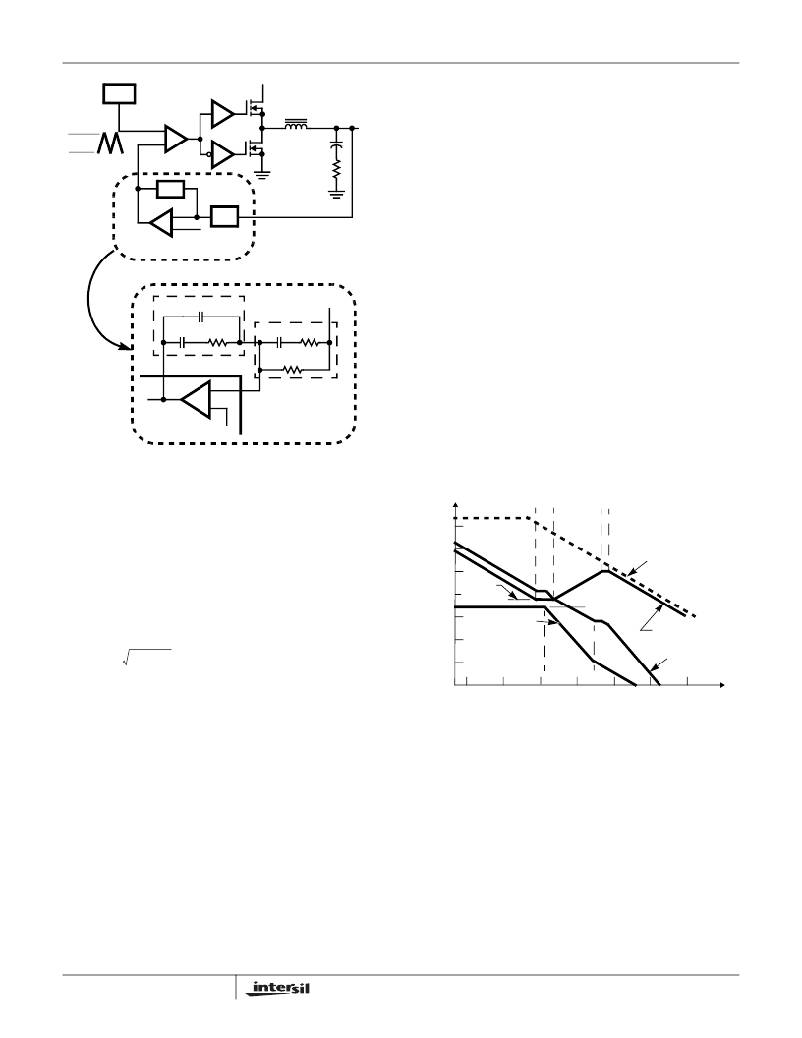
�Figure� 8� shows� an� asymptotic� plot� of� the� DC-DC� converter’s�
�-�
�+�
�ERROR�
�AMP�
�Z� IN�
�REFERENCE�
�gain� vs.� frequency.� The� actual� Modulator� Gain� has� a� high� gain�
�peak� due� to� the� high� Q� factor� of� the� output� filter� and� is� not�
�shown� in� Figure� 8.� Using� the� above� guidelines� should� give� a�
�DETAILED� COMPENSATION� COMPONENTS�
�Compensation� Gain� similar� to� the� curve� plotted.� The� open�
�loop� error� amplifier� gain� bounds� the� compensation� gain.�
�C� 1�
�C� 2�
�R� 2�
�Z� FB�
�C� 3�
�Z� IN�
�R� 3�
�V� OUT�
�Check� the� compensation� gain� at� F� P2� with� the� capabilities� of�
�the� error� amplifier.� The� Closed� Loop� Gain� is� constructed� on�
�the� log-log� graph� of� Figure� 8� by� adding� the� Modulator� Gain� (in�
�dB)� to� the� Compensation� Gain� (in� dB).� This� is� equivalent� to�
�COMP�
�HIP6004E�
�-�
�+�
�DACOUT�
�FB�
�R� 1�
�multiplying� the� modulator� transfer� function� to� the�
�compensation� transfer� function� and� plotting� the� gain.�
�The� compensation� gain� uses� external� impedance� networks�
�Z� FB� and� Z� IN� to� provide� a� stable,� high� bandwidth� (BW)� overall�
�loop.� A� stable� control� loop� has� a� gain� crossing� with�
�-20dB/decade� slope� and� a� phase� margin� greater� than� 45�
�FIGURE� 7.� VOLTAGE-MODE� BUCK� CONVERTER�
�COMPENSATION� DESIGN�
�degrees.� Include� worst� case� component� variations� when�
�determining� phase� margin.�
�The� PWM� wave� is� smoothed� by� the� output� filter� (L� O� and� C� O� ).�
�The� modulator� transfer� function� is� the� small-signal� transfer�
�function� of� V� OUT� /V� E/A� .� This� function� is� dominated� by� a� DC�
�Gain� and� the� output� filter� (L� O� and� C� O� ),� with� a� double� pole�
�break� frequency� at� F� LC� and� a� zero� at� F� ESR� .� The� DC� Gain� of�
�the� modulator� is� simply� the� input� voltage� (V� IN� )� divided� by� the�
�peak-to-peak� oscillator� voltage� ?� V� OSC� .�
�100�
�80�
�60�
�40�
�20�
�20LOG�
�(R� 2� /R� 1� )�
�F� Z1� F� Z2�
�F� P1�
�F� P2�
�OPEN� LOOP�
�ERROR� AMP� GAIN�
�20LOG�
�F� LC� =� -------------------------------------------�
�F� ESR� =� --------------------------------------------�
�MODULATOR�
�GAIN�
�F� LC�
�Modulator� Break� Frequency� Equations�
�1� 1�
�2� π� x� LO� x� CO� 2� π� x� ESR� x� C� O�
�The� compensation� network� consists� of� the� error� amplifier�
�(internal� to� the� HIP6004E)� and� the� impedance� networks� Z� IN�
�and� Z� FB� .� The� goal� of� the� compensation� network� is� to� provide�
�a� closed� loop� transfer� function� with� the� highest� 0dB� crossing�
�frequency� (f� 0dB� )� and� adequate� phase� margin.� Phase� margin�
�is� the� difference� between� the� closed� loop� phase� at� f� 0dB� and�
�180� degrees� .� The� equations� below� relate� the� compensation�
�network’s� poles,� zeros� and� gain� to� the� components� (R� 1� ,� R� 2� ,�
�R� 3� ,� C� 1� ,� C� 2� ,� and� C� 3� )� in� Figure� 7.� Use� these� guidelines� for�
�locating� the� poles� and� zeros� of� the� compensation� network:�
�(V� IN� /� ?� V� OSC� )�
�0�
�COMPENSATION�
�-20� GAIN�
�CLOSED� LOOP�
�-40� GAIN�
�F� ESR�
�-60�
�10� 100� 1K� 10K� 100K� 1M� 10M�
�FREQUENCY� (Hz)�
�FIGURE� 8.� ASYMPTOTIC� BODE� PLOT� OF� CONVERTER� GAIN�
�Component� Selection� Guidelines�
�Output� Capacitor� Selection�
�An� output� capacitor� is� required� to� filter� the� output� and� supply�
�the� load� transient� current.� The� filtering� requirements� are� a�
�function� of� the� switching� frequency� and� the� ripple� current.�
�1.�
�2.�
�3.�
�4.�
�5.�
�6.�
�7.�
�Pick� Gain� (R� 2� /R� 1� )� for� desired� converter� bandwidth.�
�Place� 1� ST� Zero� Below� Filter’s� Double� Pole� (~75%� F� LC� ).�
�Place� 2� ND� Zero� at� Filter’s� Double� Pole.�
�Place� 1� ST� Pole� at� the� ESR� Zero.�
�Place� 2� ND� Pole� at� Half� the� Switching� Frequency.�
�Check� Gain� against� Error� Amplifier’s� Open-Loop� Gain.�
�Estimate� Phase� Margin� -� Repeat� if� Necessary.�
�The� load� transient� requirements� are� a� function� of� the� slew�
�rate� (di/dt)� and� the� magnitude� of� the� transient� load� current.�
�These� requirements� are� generally� met� with� a� mix� of�
�capacitors� and� careful� layout.�
�Modern� microprocessors� produce� transient� load� rates� above�
�1A/ns.� High� frequency� capacitors� initially� supply� the� transient�
�and� slow� the� current� load� rate� seen� by� the� bulk� capacitors.�
�8�
�相关PDF资料 |
PDF描述 |
|---|---|
| HIP6004BCB | IC CTRLR PWM VOLTAGE MON 20-SOIC |
| UVK2V3R3MPD | CAP ALUM 3.3UF 350V 20% RADIAL |
| AHA476M50X16T-F | CAP ALUM 47UF 50V 20% SMD |
| HIP6004ECB-T | IC CTRLR PWM VOLTAGE MON 20-SOIC |
| AHA336M50X16T-F | CAP ALUM 33UF 50V 20% SMD |
相关代理商/技术参数 |
参数描述 |
|---|---|
| HIP6004ECV-T | 功能描述:IC CTRLR PWM VOLTAGE MON 20TSSOP RoHS:否 类别:集成电路 (IC) >> PMIC - 稳压器 - 专用型 系列:- 产品培训模块:Lead (SnPb) Finish for COTS Obsolescence Mitigation Program 标准包装:2,000 系列:- 应用:电源,ICERA E400,E450 输入电压:4.1 V ~ 5.5 V 输出数:10 输出电压:可编程 工作温度:-40°C ~ 85°C 安装类型:表面贴装 封装/外壳:42-WFBGA,WLCSP 供应商设备封装:42-WLP 包装:带卷 (TR) |
| HIP6004ECVZ | 功能描述:电压模式 PWM 控制器 20LD BUCK & SYNCHCT PWMCONT & OUTPUT RoHS:否 制造商:Texas Instruments 输出端数量:1 拓扑结构:Buck 输出电压:34 V 输出电流: 开关频率: 工作电源电压:4.5 V to 5.5 V 电源电流:600 uA 最大工作温度:+ 125 C 最小工作温度:- 40 C 封装 / 箱体:WSON-8 封装:Reel |
| HIP6004ECVZ-T | 功能描述:电压模式 PWM 控制器 20LD BUCK&SYNCHCT PWMCONOUTPUT RoHS:否 制造商:Texas Instruments 输出端数量:1 拓扑结构:Buck 输出电压:34 V 输出电流: 开关频率: 工作电源电压:4.5 V to 5.5 V 电源电流:600 uA 最大工作温度:+ 125 C 最小工作温度:- 40 C 封装 / 箱体:WSON-8 封装:Reel |
| HIP6004EVAL1 | 功能描述:EVALUATION BOARD HIP6004 RoHS:否 类别:编程器,开发系统 >> 过时/停产零件编号 系列:- 标准包装:1 系列:- 传感器类型:CMOS 成像,彩色(RGB) 传感范围:WVGA 接口:I²C 灵敏度:60 fps 电源电压:5.7 V ~ 6.3 V 嵌入式:否 已供物品:成像器板 已用 IC / 零件:KAC-00401 相关产品:4H2099-ND - SENSOR IMAGE WVGA COLOR 48-PQFP4H2094-ND - SENSOR IMAGE WVGA MONO 48-PQFP |
| HIP6004EVAL3 | 功能描述:电源管理IC开发工具 EMBEDDED EVAL BRD SYNC BUCK/KLAM RoHS:否 制造商:Maxim Integrated 产品:Evaluation Kits 类型:Battery Management 工具用于评估:MAX17710GB 输入电压: 输出电压:1.8 V |
发布紧急采购,3分钟左右您将得到回复。