参数资料
| 型号: | HIP6012CV-T |
| 厂商: | Intersil |
| 文件页数: | 7/12页 |
| 文件大小: | 0K |
| 描述: | IC CTRLR PWM SYNC BUCK 14-TSSOP |
| 标准包装: | 2,500 |
| 应用: | 控制器,Intel Pentium? Pro、PowerP、Alpha |
| 输入电压: | 5V,12V |
| 输出数: | 1 |
| 输出电压: | 1.3 V ~ 12 V |
| 工作温度: | 0°C ~ 70°C |
| 安装类型: | * |
| 封装/外壳: | 14-TSSOP(0.173",4.40mm 宽) |
| 供应商设备封装: | * |
| 包装: | 带卷 (TR) |
�� �
�
�HIP6012�
�V� IN�
�5.� Place� 2� ND� Pole� at� Half� the� Switching� Frequency�
�OSC�
�DRIVER�
�6.� Check� Gain� against� Error� Amplifier’s� Open-Loop� Gain�
�?� V� OSC�
�PWM�
�COMPARATOR�
�-�
�+�
�DRIVER�
�L� O�
�PHASE�
�C� O�
�ESR�
�(PARASITIC)�
�V� OUT�
�7.� Estimate� Phase� Margin� -� Repeat� if� Necessary�
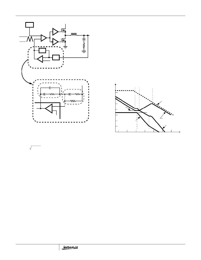
�Figure� 8� shows� an� asymptotic� plot� of� the� DC-DC� converter’s�
�gain� vs� frequency.� The� actual� Modulator� Gain� has� a� high� gain�
�peak� do� to� the� high� Q� factor� of� the� output� filter� and� is� not� shown�
�in� Figure� 8.� Using� the� above� guidelines� should� give� a�
�V� E/A�
�Z� FB�
�Compensation� Gain� similar� to� the� curve� plotted.� The� open� loop�
�error� amplifier� gain� bounds� the� compensation� gain.� Check� the�
�-�
�+�
�ERROR�
�AMP�
�Z� IN�
�REFERENCE�
�compensation� gain� at� F� P2� with� the� capabilities� of� the� error�
�amplifier.� The� Closed� Loop� Gain� is� constructed� on� the� log-log�
�graph� of� Figure� 8� by� adding� the� Modulator� Gain� (in� dB)� to� the�
�Compensation� Gain� (in� dB).� This� is� equivalent� to� multiplying� the�
�DETAILED� COMPENSATION� COMPONENTS�
�modulator� transfer� function� to� the� compensation� transfer�
�function� and� plotting� the� gain.�
�C1�
�C2�
�R2�
�Z� FB�
�C3�
�Z� IN�
�R3�
�V� OUT�
�100�
�80�
�F� Z1� F� Z2�
�F� P1�
�F� P2�
�COMP�
�-�
�FB�
�R1�
�60�
�40�
�20LOG�
�OPEN� LOOP�
�ERROR� AMP� GAIN�
�+�
�20�
�(R2/R1)�
�20LOG�
�HIP6012�
�REF�
�0�
�-20�
�MODULATOR�
�(V� IN� /� ?� V� OSC� )�
�COMPENSATION�
�GAIN�
�FIGURE� 7.� VOLTAGE� -� MODE� BUCK� CONVERTER�
�COMPENSATION� DESIGN�
�-40�
�-60�
�10�
�100�
�GAIN�
�1K�
�F� LC�
�10K�
�F� ESR�
�100K�
�1M�
�CLOSED� LOOP�
�GAIN�
�10M�
�Modulator� Break� Frequency� Equations�
�FREQUENCY� (Hz)�
�F� LC� =� ---------------------------------------�
�F� ESR� =� ---------------------------------------------�
�1�
�2� π� ?� L� O� ?� C� O�
�1�
�2� π� ?� (� ESR� ?� C� O� )�
�FIGURE� 8.� ASYMPTOTIC� BODE� PLOT� OF� CONVERTER� GAIN�
�The� compensation� gain� uses� external� impedance� networks�
�The� compensation� network� consists� of� the� error� amplifier�
�(internal� to� the� HIP6012)� and� the� impedance� networks� Z� IN�
�and� Z� FB� .� The� goal� of� the� compensation� network� is� to� provide�
�a� closed� loop� transfer� function� with� the� highest� 0dB� crossing�
�frequency� (f� 0dB� )� and� adequate� phase� margin.� Phase� margin�
�is� the� difference� between� the� closed� loop� phase� at� f� 0dB� and�
�180� o� .� The� equations� below� relate� the� compensation�
�network’s� poles,� zeros� and� gain� to� the� components� (R1,� R2,�
�R3,� C1,� C2,� and� C3)� in� Figure� 8.� Use� these� guidelines� for�
�locating� the� poles� and� zeros� of� the� compensation� network:�
�Compensation� Break� Frequency� Equations�
�Z� FB� and� Z� IN� to� provide� a� stable,� high� bandwidth� (BW)� overall�
�loop.� A� stable� control� loop� has� a� gain� crossing� with�
�-20dB/decade� slope� and� a� phase� margin� greater� than� 45� o� .�
�Include� worst� case� component� variations� when� determining�
�phase� margin.�
�Component� Selection� Guidelines�
�Output� Capacitor� Selection�
�An� output� capacitor� is� required� to� filter� the� output� and� supply�
�the� load� transient� current.� The� filtering� requirements� are� a�
�function� of� the� switching� frequency� and� the� ripple� current.�
�F� Z1� =� ----------------------------------�
�F� P1� =� -------------------------------------------------------�
�2� π� ?� R2� ?� ?� ----------------------� ?�
�F� Z2� =� ------------------------------------------------------�
�F� P2� =� ----------------------------------�
�1�
�2� π� ?� R� 2� ?� C1�
�1�
�2� π� ?� (� R1� +� R3� )� ?� C3�
�1�
�C1� ?� C2�
�?� C1� +� C2� ?�
�1�
�2� π� ?� R3� ?� C3�
�The� load� transient� requirements� are� a� function� of� the� slew�
�rate� (di/dt)� and� the� magnitude� of� the� transient� load� current.�
�These� requirements� are� generally� met� with� a� mix� of�
�capacitors� and� careful� layout.�
�1.� Pick� Gain� (R2/R1)� for� desired� converter� bandwidth�
�2.� Place� 1� ST� Zero� Below� Filter’s� Double� Pole�
�(~75%� F� LC� )�
�3.� Place� 2� ND� Zero� at� Filter’s� Double� Pole�
�4.� Place� 1� ST� Pole� at� the� ESR� Zero�
�7�
�Modern� microprocessors� produce� transient� load� rates� above�
�1A/ns.� High� frequency� capacitors� initially� supply� the� transient�
�and� slow� the� current� load� rate� seen� by� the� bulk� capacitors.�
�The� bulk� filter� capacitor� values� are� generally� determined� by�
�the� ESR� (effective� series� resistance)� and� voltage� rating�
�requirements� rather� than� actual� capacitance� requirements.�
�FN4324.2�
�December� 27,� 2004�
�相关PDF资料 |
PDF描述 |
|---|---|
| HIP6013CB-T | IC CONTROLLER PWM BUCK 14-SOIC |
| HIP6301CB | IC REG CTRLR BUCK PWM 20-SOIC |
| HIP6302CB | IC REG CTRLR BUCK PWM 16-SOIC |
| HIP6302VCB-T | IC REG CTRLR BUCK PWM 16-SOIC |
| HIP6303CB-T | IC REG CTRLR BUCK PWM 20-SOIC |
相关代理商/技术参数 |
参数描述 |
|---|---|
| HIP6012CVZ | 制造商:INTERSIL 制造商全称:Intersil Corporation 功能描述:Buck and Synchronous-Rectifier Pulse-Width Modulator (PWM) Controller |
| HIP6012EVAL1 | 功能描述:电源管理IC开发工具 DISK DRIVE SUPPLY EVAL BRD RoHS:否 制造商:Maxim Integrated 产品:Evaluation Kits 类型:Battery Management 工具用于评估:MAX17710GB 输入电压: 输出电压:1.8 V |
| HIP6013 | 制造商:INTERSIL 制造商全称:Intersil Corporation 功能描述:Buck Pulse-Width Modulator (PWM) Controller |
| HIP6013_05 | 制造商:INTERSIL 制造商全称:Intersil Corporation 功能描述:Buck Pulse-Width Modulator (PWM) Controller |
| HIP6013CB | 功能描述:电流型 PWM 控制器 Buck PWM RoHS:否 制造商:Texas Instruments 开关频率:27 KHz 上升时间: 下降时间: 工作电源电压:6 V to 15 V 工作电源电流:1.5 mA 输出端数量:1 最大工作温度:+ 105 C 安装风格:SMD/SMT 封装 / 箱体:TSSOP-14 |
发布紧急采购,3分钟左右您将得到回复。