- 您现在的位置:买卖IC网 > Datasheet目录40 > HIP6018BCBZ-T (Intersil)IC REG TRPL BCK/LINEAR 24-SOIC Datasheet资料下载
参数资料
| 型号: | HIP6018BCBZ-T |
| 厂商: | Intersil |
| 文件页数: | 11/15页 |
| 文件大小: | 384K |
| 描述: | IC REG TRPL BCK/LINEAR 24-SOIC |
| 标准包装: | 1,000 |
| 拓扑: | 降压(降压)同步(1),线性(LDO)(2) |
| 功能: | 任何功能 |
| 输出数: | 3 |
| 频率 - 开关: | 215kHz |
| 电压/电流 - 输出 1: | 控制器 |
| 电压/电流 - 输出 2: | 2.5V,- |
| 电压/电流 - 输出 3: | 控制器 |
| 带 LED 驱动器: | 无 |
| 带监控器: | 无 |
| 带序列发生器: | 无 |
| 电源电压: | 3.3 V ~ 12 V |
| 工作温度: | 0°C ~ 70°C |
| 安装类型: | * |
| 封装/外壳: | 24-SOIC(0.295",7.50mm 宽) |
| 供应商设备封装: | * |
| 包装: | 带卷 (TR) |
11
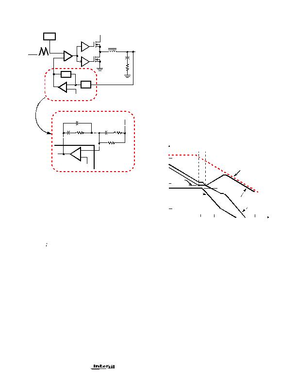
The modulator transfer function is the small-signal transfer
function of V
OUT
/V
E/A
. This function is dominated by a DC
gain and the output filter, with a double pole break frequency
at F
LC
and a zero at F
ESR
. The DC gain of the modulator is
simply the input voltage, V
IN
, divided by the peak-to-peak
oscillator voltage, 擵
OSC
.
Modulator Break Frequency Equations
The compensation network consists of the error amplifier
internal to the HIP6018B and the impedance networks Z
IN
and
Z
FB
. The goal of the compensation network is to provide a
closed loop transfer function with an acceptable 0dB crossing
frequency (f
0dB
) and adequate phase margin. Phase margin is
the difference between the closed loop phase at f
0dB
and 180
degrees. The equations below relate the compensation
networks poles, zeros and gain to the components (R1, R2,
R3, C1, C2, and C3) in Figure 11. Use these guidelines for
locating the poles and zeros of the compensation network:
1. Pick Gain (R2/R1) for desired converter bandwidth
2. Place 1
ST
Zero Below Filters Double Pole (~75% F
LC
)
3. Place 2
ND
Zero at Filters Double Pole
4. Place 1
ST
Pole at the ESR Zero
5. Place 2
ND
Pole at Half the Switching Frequency
6. Check Gain against Error Amplifiers Open-Loop Gain
7. Estimate Phase Margin - Repeat if Necessary
Compensation Break Frequency Equations
Figure 12 shows an asymptotic plot of the DC-DC converters
gain vs. frequency. The actual modulator gain has a peak due
to the high Q factor of the output filter at F
LC
, which is not
shown in Figure 12. Using the above guidelines should yield a
compensation gain similar to the curve plotted. The open loop
error amplifier gain bounds the compensation gain. Check the
compensation gain at F
P2
with the capabilities of the error
amplifier. The closed loop gain is constructed on the log-log
graph of Figure 12 by adding the modulator gain (in dB) to the
compensation gain (in dB). This is equivalent to multiplying
the modulator transfer function to the compensation transfer
function and plotting the gain.
The compensation gain uses external impedance networks
Z
FB
and Z
IN
to provide a stable, high bandwidth loop. A
stable control loop has a 0dB gain crossing with
-20dB/decade slope and a phase margin greater than 45
degrees. Include worst case component variations when
determining phase margin.
Component Selection Guidelines
Output Capacitor Selection
The output capacitors for each output have unique
requirements. In general the output capacitors should be
selected to meet the dynamic regulation requirements.
Additionally, the PWM converters require an output
capacitor to filter the current ripple. The linear regulator is
internally compensated and requires an output capacitor that
meets the stability requirements. The load transient for the
microprocessor core requires high quality capacitors to
supply the high slew rate (di/dt) current demands.
FIGURE 11. VOLTAGE-MODE BUCK CONVERTER
COMPENSATION DESIGN
V
OUT
OSC
REFERENCE
L
O
C
O
ESR
V
IN
?SPAN class="pst HIP6018BCBZ-T_2462225_6">V
OSC
ERROR
AMP
PWM
DRIVER
(PARASITIC)
Z
FB
+
-
REFERENCE
R1
R3
R2
C3
C2
C1
COMP
V
OUT
FB
Z
FB
HIP6018B
Z
IN
COMP
DRIVER
DETAILED FEEDBACK COMPENSATION
PHASE
V
E/A
+
-
+
-
Z
IN
F
LC
1
2?nbsp L
O
C
O
?/DIV>
?/DIV>
----------------------------------------
=
F
ESR
1
2?ESR C
O
?/DIV>
?/DIV>
-----------------------------------------
=
F
Z1
1
2?R
?2 C1
?/DIV>
-----------------------------------
=
F
Z2
1
2?nbsp R1 R3
+
( ) C3
?/DIV>
?/DIV>
-------------------------------------------------------
=
F
P1
1
2?R
2
C1 C2
?/DIV>
C1 C2
+
----------------------
?nbsp ?/DIV>
?nbsp ?/DIV>
?/DIV>
?/DIV>
-------------------------------------------------------
=
F
P2
1
2?R
?3 C3
?/DIV>
-----------------------------------
=
100
80
60
40
20
0
-20
-40
-60
F
P1
F
Z2
10M
1M
100K
10K
1K
100
10
OPEN LOOP
ERROR AMP GAIN
F
Z1
F
P2
20LOG
F
LC
F
ESR
COMPENSATION
FREQUENCY (Hz)
GAIN
20LOG
(V
IN
/?/SPAN>V
OSC
)
MODULATOR
GAIN
(R
2
/R
1
)
FIGURE 12. ASYMPTOTIC BODE PLOT OF CONVERTER GAIN
CLOSED LOOP
GAIN
HIP6018B
相关PDF资料 |
PDF描述 |
|---|---|
| HIP6021CB-T | IC REG QD BCK/LINEAR 28-SOIC |
| HIP6521CB-T | IC REG QD BCK/LINEAR SYNC 16SOIC |
| HMC920LP5E | IC CTRLR ACTIVE BIAS 32QFN |
| IDTTSE2002B3CNRG | IC TEMP SENS EEPROM DFN-8 |
| IPM6220ACAZ-T | IC REG 5OUT BUCK/LDO SYNC 24SSOP |
相关代理商/技术参数 |
参数描述 |
|---|---|
| HIP6018CB | 制造商:Rochester Electronics LLC 功能描述:- Bulk 制造商:Harris Corporation 功能描述: |
| HIP6018CB-T | 制造商:Rochester Electronics LLC 功能描述:- Tape and Reel |
| HIP6018EVAL1 | 制造商:INTERSIL 制造商全称:Intersil Corporation 功能描述:Advanced PWM and Dual Linear Power Control |
| HIP6019 | 制造商:IRF 制造商全称:International Rectifier 功能描述:5-BIT PROGRAMMABLE SYNCHRONOUS BUCK, NON-SYNCHRONOUS,ADJUSTABLE LDO AND 200mA ON-BOARD LDO |
| HIP6019B | 制造商:INTERSIL 制造商全称:Intersil Corporation 功能描述:Advanced Dual PWM and Dual Linear Power Control |
发布紧急采购,3分钟左右您将得到回复。