- 您现在的位置:买卖IC网 > PDF目录371821 > HIP6019BCB (HARRIS SEMICONDUCTOR) Advanced Dual PWM and Dual Linear Power Control PDF资料下载
参数资料
| 型号: | HIP6019BCB |
| 厂商: | HARRIS SEMICONDUCTOR |
| 元件分类: | 稳压器 |
| 英文描述: | Advanced Dual PWM and Dual Linear Power Control |
| 中文描述: | DUAL SWITCHING CONTROLLER, 1000 kHz SWITCHING FREQ-MAX, PDSO28 |
| 封装: | SOIC-28 |
| 文件页数: | 13/15页 |
| 文件大小: | 362K |
| 代理商: | HIP6019BCB |
279
The response time to a transient is different for the
application of load and the removal of load. The following
equations give the approximate response time interval for
application and removal of a transient load:
where: I
TRAN
is the transient load current step, t
RISE
is the
response time to the application of load, and t
FALL
is the
response time to the removal of load. With a +5V input
source, the worst case response time can be either at the
application or removal of load and dependent upon the
output voltage setting. Be sure to check both of these
equations at the minimum and maximum output levels for
the worst case response time.
Input Capacitor Selection
The important parameters for the bulk input capacitor are the
voltage rating and the RMS current rating. For reliable
operation, select the bulk capacitor with voltage and current
ratings above the maximum input voltage and largest RMS
current required by the circuit. The capacitor voltage rating
should be at least 1.25 times greater than the maximum
input voltage and a voltage rating of 1.5 times is a
conservative guideline.
Use a mix of input bypass capacitors to control the voltage
overshoot across the MOSFETs. Use ceramic capacitance
for the high frequency decoupling and bulk capacitors to
supply the RMS current. Small ceramic capacitors should be
placed very close to the upper MOSFET to suppress the
voltage induced in the parasitic circuit impedances.
For a through hole design, several electrolytic capacitors
(Panasonic HFQ series or Nichicon PL series or Sanyo MV-
GX or equivalent) may be needed. For surface mount
designs, solid tantalum capacitors can be used, but caution
must be exercised with regard to the capacitor surge current
rating. These capacitors must be capable of handling the
surge-current at power-up. The TPS series available from
AVX, and the 593D series from Sprague are both surge
current tested.
MOSFET Selection/Considerations
The HIP6019B requires 4 N-Channel power MOSFETs. Two
MOSFETs are used in the synchronous-rectified buck
topology of PWM1 converter. PWM2 converter uses a
MOSFET as the buck switch and the linear controller drives
a MOSFET as a pass transistor. These should be selected
based upon r
DS(ON)
, gate supply requirements, and thermal
management requirements.
PWM1 MOSFET Selection and Considerations
In high-current PWM applications, the MOSFET power
dissipation, package selection and heatsink are the
dominant design factors. The power dissipation includes two
loss components; conduction loss and switching loss. These
losses are distributed between the upper and lower
MOSFETs according to duty factor (see the equations
below). The conduction losses are the only component of
power dissipation for the lower MOSFETs. Only the upper
MOSFET has switching losses, since the lower device turns
on into near zero voltage.
The equations below assume linear voltage-current
transitions and do not model power loss due to the reverse-
recovery of the lower MOSFET’s body diode. The gate-
charge losses are proportional to the switching frequency
(F
S
) and are dissipated by the HIP6019B, thus not
contributing to the MOSFETs’ temperature rise. However,
large gate charge increases the switching interval, t
SW
which increases the upper MOSFET switching losses.
Ensure that both MOSFETs are within their maximum
junction temperature at high ambient temperature by
calculating the temperature rise according to package
thermal resistance specifications. A separate heatsink may
be necessary depending upon MOSFET power, package
type, ambient temperature and air flow.
The r
DS(ON)
is different for the two previous equations even
if the type device is used for both. This is because the gate
drive applied to the upper MOSFET is different than the
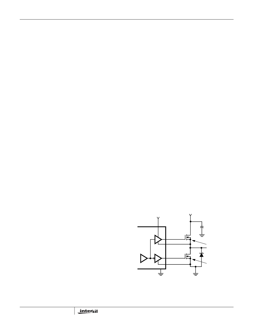
lower MOSFET. Figure 14 shows the gate drive where the
upper gate-to-source voltage is approximately V
CC
less the
input supply. For +5V main power and +12V
DC
for the bias,
the gate-to-source voltage of Q1 is 7V. The lower gate drive
voltage is +12V
DC
. A logic-level MOSFET is a good choice
for Q1 and a logic-level MOSFET can be used for Q2 if its
absolute gate-to-source voltage rating exceeds the
maximum voltage applied to V
CC
.
Rectifier CR1 is a clamp that catches the negative inductor
swing during the dead time between the turn off of the
t
RISE
L
IN
I
OUT
×
----------–
=
t
FALL
L
------------------------------
I
OUT
×
=
P
UPPER
I
------------------------------------------------------------
2
r
IN
r
×
V
×
I
----------------------------------------------------
V
×
t
×
F
S
×
+
=
P
LOWER
I
--------------------------------------------------------------------------------
2
IN
×
V
V
–
(
)
×
=
+12V
PGND
HIP6019B
GND
LGATE
UGATE
PHASE
V
CC
+5V OR LESS
NOTE:
V
GS
≈
V
CC
-5V
NOTE:
V
GS
≈
V
CC
Q1
Q2
+
-
FIGURE 14. OUTPUT GATE DRIVERS
CR1
HIP6019B
相关PDF资料 |
PDF描述 |
|---|---|
| HIP6019B | FPGA - 100000 SYSTEM GATE 2.5 VOLT - NOT RECOMMENDED for NEW DESIGN |
| HIP6028EVAL1 | Advanced PWM and Dual Linear Power Control with Integrated ACPI Support Interface |
| HIP6028 | Advanced PWM and Dual Linear Power Control with Integrated ACPI Support Interface |
| HIP6028CB | Advanced PWM and Dual Linear Power Control with Integrated ACPI Support Interface |
| HIP6303CB-T | Microprocessor CORE Voltage Regulator Multi-Phase Buck PWM Controller |
相关代理商/技术参数 |
参数描述 |
|---|---|
| HIP6019BCB-T | 功能描述:IC REG QD BCK/LINEAR 28-SOIC RoHS:否 类别:集成电路 (IC) >> PMIC - 稳压器 - 线性 + 切换式 系列:- 标准包装:2,500 系列:- 拓扑:降压(降压)同步(3),线性(LDO)(2) 功能:任何功能 输出数:5 频率 - 开关:300kHz 电压/电流 - 输出 1:控制器 电压/电流 - 输出 2:控制器 电压/电流 - 输出 3:控制器 带 LED 驱动器:无 带监控器:无 带序列发生器:是 电源电压:5.6 V ~ 24 V 工作温度:-40°C ~ 85°C 安装类型:* 封装/外壳:* 供应商设备封装:* 包装:* |
| HIP6019BCBZ | 功能描述:电压模式 PWM 控制器 ADV DL 3PWM & DL LINER PWR CONTROL RoHS:否 制造商:Texas Instruments 输出端数量:1 拓扑结构:Buck 输出电压:34 V 输出电流: 开关频率: 工作电源电压:4.5 V to 5.5 V 电源电流:600 uA 最大工作温度:+ 125 C 最小工作温度:- 40 C 封装 / 箱体:WSON-8 封装:Reel |
| HIP6019BCBZ-T | 功能描述:电压模式 PWM 控制器 ADV DL 3PWM & DL LINER PWR CONTROL RoHS:否 制造商:Texas Instruments 输出端数量:1 拓扑结构:Buck 输出电压:34 V 输出电流: 开关频率: 工作电源电压:4.5 V to 5.5 V 电源电流:600 uA 最大工作温度:+ 125 C 最小工作温度:- 40 C 封装 / 箱体:WSON-8 封装:Reel |
| HIP6019BEVAL1 | 功能描述:电源管理IC开发工具 HIP6019B EVAL BRD FOR MB PWR MGMT RoHS:否 制造商:Maxim Integrated 产品:Evaluation Kits 类型:Battery Management 工具用于评估:MAX17710GB 输入电压: 输出电压:1.8 V |
| HIP6019CB | 制造商:Harris Corporation 功能描述: |
发布紧急采购,3分钟左右您将得到回复。