- 您现在的位置:买卖IC网 > PDF目录22322 > HIP6019BCBZ-T (Intersil)IC REG QD BCK/LINEAR 28-SOIC PDF资料下载
参数资料
| 型号: | HIP6019BCBZ-T |
| 厂商: | Intersil |
| 文件页数: | 7/15页 |
| 文件大小: | 0K |
| 描述: | IC REG QD BCK/LINEAR 28-SOIC |
| 标准包装: | 1,000 |
| 拓扑: | 降压(降压)同步(2),线性(LDO)(2) |
| 功能: | 任何功能 |
| 输出数: | 4 |
| 频率 - 开关: | 215kHz |
| 电压/电流 - 输出 1: | 控制器 |
| 电压/电流 - 输出 2: | 控制器 |
| 电压/电流 - 输出 3: | 控制器 |
| 带 LED 驱动器: | 无 |
| 带监控器: | 无 |
| 带序列发生器: | 无 |
| 电源电压: | 5 V ~ 12 V |
| 工作温度: | 0°C ~ 70°C |
| 安装类型: | * |
| 封装/外壳: | 28-SOIC(0.295",7.50mm 宽) |
| 供应商设备封装: | * |
| 包装: | 带卷 (TR) |
�� �
�
�HIP6019B�
�Description�
�Operation�
�The� HIP6019B� monitors� and� precisely� controls� 4� output�
�voltage� levels� (Refer� to� Figures� 1,� 2,� and� 3).� It� is� designed�
�for� microprocessor� computer� applications� with� 5V� power� and�
�12V� bias� input� from� a� PS2� or� ATX� power� supply.� The� IC� has�
�2� PWM� controllers,� a� linear� controller,� and� a� linear� regulator.�
�The� first� PWM� controller� (PWM1)� is� designed� to� regulate� the�
�microprocessor� core� voltage� (V� OUT1� ).� PWM1� controller�
�drives� 2� MOSFETs� (Q1� and� Q2)� in� a� synchronous-rectified�
�buck� converter� configuration� and� regulates� the� core� voltage�
�to� a� level� programmed� by� the� 5-bit� digital-to-analog�
�converter� (DAC).� The� second� PWM� controller� (PWM2)� is�
�designed� to� regulate� the� I/O� voltage� (V� OUT2� ).� PWM2�
�controller� drives� a� MOSFET� (Q3)� in� a� standard� buck�
�converter� configuration� and� regulates� the� I/O� voltage� to� a�
�resistor� programmable� level� between� 3.0� and� 3.5V� DC� .� An�
�integrated� linear� regulator� supplies� the� 2.5V� clock� generator�
�power� (V� OUT4� ).� The� linear� controller� drives� an� external�
�increases,� the� pulse-width� on� the� PHASE� pin� increases.� The�
�interval� of� increasing� pulse-width� continues� until� each� output�
�reaches� sufficient� voltage� to� transfer� control� to� the� input�
�reference� clamp.� If� we� consider� the� 3.3V� output� (V� OUT2� )� in�
�Figure� 6,� this� time� occurs� at� T2.� During� the� interval� between�
�T2� and� T3,� the� error� amplifier� reference� ramps� to� the� final�
�value� and� the� converter� regulates� the� output� to� a� voltage�
�proportional� to� the� SS� pin� voltage.� At� T3� the� input� clamp�
�voltage� exceeds� the� reference� voltage� and� the� output� voltage�
�is� in� regulation.�
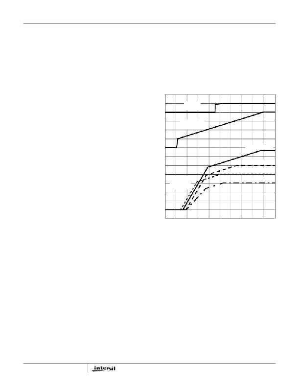
�PGOOD�
�(2V/DIV)�
�0V�
�SOFT-START�
�(1V/DIV)�
�MOSFET� (Q4)� to� supply� the� GTL� bus� power� (V� OUT3� ).�
�Initialization�
�The� HIP6019B� automatically� initializes� upon� receipt� of� input�
�power.� Special� sequencing� of� the� input� supplies� is� not�
�necessary.� The� Power-On� Reset� (POR)� function� continually�
�monitors� the� input� supply� voltages.� The� POR� monitors� the�
�bias� voltage� (+12V� IN� )� at� the� VCC� pin� and� the� 5V� input�
�voltage� (+5V� IN� )� at� the� OCSET1� pin.� The� normal� level� on�
�OCSET1� is� equal� to� +5V� IN� less� a� fixed� voltage� drop� (see�
�over-current� protection).� The� POR� function� initiates� soft-start�
�operation� after� both� input� supply� voltages� exceed� their� POR�
�thresholds.�
�0V�
�0V�
�OUTPUT�
�VOLTAGES�
�(0.5V/DIV)�
�V� OUT2� ( = 3.3V)�
�V� OUT4� (� =� 2.5V)�
�V� OUT1� (DAC = 2V)�
�V� OUT3� (� =� 1.5V)�
�T0� T1�
�T2�
�T3�
�Soft-Start�
�The� POR� function� initiates� the� soft-start� sequence.� Initially,�
�the� voltage� on� the� SS� pin� rapidly� increases� to� approximately�
�1V� (this� minimizes� the� soft-start� interval).� Then� an� internal�
�11� μ� A� current� source� charges� an� external� capacitor� (C� SS� )� on�
�the� SS� pin� to� 4V.� The� PWM� error� amplifier� reference� inputs�
�(+� terminal)� and� outputs� (COMP1� and� COMP2� pins)� are�
�clamped� to� a� level� proportional� to� the� SS� pin� voltage.� As� the�
�SS� pin� voltage� ramps� from� 1V� to� 4V,� the� output� clamp� allows�
�generation� of� PHASE� pulses� of� increasing� width� that� charge�
�the� output� capacitor(s).� After� this� initial� stage,� the� reference�
�input� clamp� slows� the� output� voltage� rate-of-rise� and�
�provides� a� smooth� transition� to� the� final� set� voltage.�
�Additionally,� both� linear� regulator’s� reference� inputs� are�
�clamped� to� a� voltage� proportional� to� the� SS� pin� voltage.� This�
�method� provides� a� rapid� and� controlled� output� voltage� rise.�
�Figure� 6� shows� the� soft-start� sequence� for� the� typical�
�application.� At� T0� the� SS� voltage� rapidly� increases� to�
�approximately� 1V.� At� T1,� the� SS� pin� and� error� amplifier� output�
�voltage� reach� the� valley� of� the� oscillator’s� triangle� wave.� The�
�oscillator’s� triangular� waveform� is� compared� to� the� clamped�
�error� amplifier� output� voltage.� As� the� SS� pin� voltage�
�7�
�TIME�
�FIGURE� 6.� SOFT-START� INTERVAL�
�The� remaining� outputs� are� also� programmed� to� follow� the�
�SS� pin� voltage.� Each� linear� output� (V� OUT3� and� V� OUT4� )�
�initially� follows� the� 3.3V� output� (V� OUT2� ).� When� each� output�
�reaches� sufficient� voltage� the� input� reference� clamp� slows�
�the� rate� of� output� voltage� rise.� The� PGOOD� signal� toggles�
�‘high’� when� all� output� voltage� levels� have� exceeded� their�
�under-voltage� levels.� See� the� Soft-Start� Interval� section�
�under� Applications� Guidelines� for� a� procedure� to� determine�
�the� soft-start� interval.�
�Fault� Protection�
�All� four� outputs� are� monitored� and� protected� against� extreme�
�overload.� A� sustained� overload� on� any� linear� regulator�
�output� or� an� over-voltage� on� the� PWM� outputs� disables� all�
�converters� and� drives� the� FAULT/RT� pin� to� VCC.�
�Figure� 7� shows� a� simplified� schematic� of� the� fault� logic.� An�
�over-voltage� detected� on� either� VSEN1� or� VSEN2�
�immediately� sets� the� fault� latch.� A� sequence� of� three� over-�
�current� fault� signals� also� sets� the� fault� latch.� A� comparator�
�FN4587.1�
�April� 13,� 2005�
�相关PDF资料 |
PDF描述 |
|---|---|
| EEC26DRYI-S13 | CONN EDGECARD 52POS .100 EXTEND |
| FMC19DRXS | CONN EDGECARD 38POS DIP .100 SLD |
| LM4040C10IDBZR | IC VREF SHUNT PREC 10V SOT-23-3 |
| EMC43DRAS | CONN EDGECARD 86POS R/A .100 SLD |
| VLCF5020T-150MR90-1 | INDUCTOR POWER 15UH .90A SMD |
相关代理商/技术参数 |
参数描述 |
|---|---|
| HIP6019BEVAL1 | 功能描述:电源管理IC开发工具 HIP6019B EVAL BRD FOR MB PWR MGMT RoHS:否 制造商:Maxim Integrated 产品:Evaluation Kits 类型:Battery Management 工具用于评估:MAX17710GB 输入电压: 输出电压:1.8 V |
| HIP6019CB | 制造商:Harris Corporation 功能描述: |
| HIP6019CB-T | 制造商:Rochester Electronics LLC 功能描述:- Bulk |
| HIP6019EVAL1 | 制造商:INTERSIL 制造商全称:Intersil Corporation 功能描述:Advanced Dual PWM and Dual Linear Power Control |
| HIP6020 | 制造商:INTERSIL 制造商全称:Intersil Corporation 功能描述:Advanced Dual PWM and Dual Linear Power Controller |
发布紧急采购,3分钟左右您将得到回复。