- 您现在的位置:买卖IC网 > PDF目录385382 > HIP6020A (Intersil Corporation) Advanced Dual PWM and Dual Linear Power Controller PDF资料下载
参数资料
| 型号: | HIP6020A |
| 厂商: | Intersil Corporation |
| 元件分类: | 基准电压源/电流源 |
| 英文描述: | Advanced Dual PWM and Dual Linear Power Controller |
| 中文描述: | 先进的双PWM和线性双电源控制器 |
| 文件页数: | 10/16页 |
| 文件大小: | 192K |
| 代理商: | HIP6020A |
4-10
Application Guidelines
Soft-Start Interval
Initially,thesoft-startfunctionclampstheerroramplifier’soutput
of the PWM converters. This generates PHASE pulses of
increasing width that charge the output capacitor(s). After the
output voltage increases to approximately 70% of the set value,
the reference input of the error amplifier is clamped to a voltage
proportionaltotheSSpinvoltage.Theresultingoutputvoltages
start-up as shown in Figure 6.
The soft-start function controls the output voltage rate of rise
to limit the current surge at start-up. The soft-start interval
and the surge current are programmed by the soft-start
capacitor, C
SS
. Programming a faster soft-start interval
increases the peak surge current. The peak surge current
occurs during the initial output voltage rise to 70% of the set
value. Using the recommended 0.1
μ
F soft start capacitor
insures all output voltages ramp up to their set values within
10ms of the input voltages reaching POR levels.
Shutdown
Neither PWM output switches until the soft-start voltage
(V
SS
) exceeds the oscillator’s valley voltage. Additionally, the
reference on each linear’s amplifier is clamped to the soft-
start voltage. Holding the SS pin low (with an open drain or
open collector signal) turns off all four regulators.
Layout Considerations
MOSFETs switch very fast and efficiently. The speed with
which the current transitions from one device to another
causes voltage spikes across the interconnecting
impedances and parasitic circuit elements. The voltage
spikes can degrade efficiency, radiate noise into the circuit,
and lead to device over-voltage stress. Careful component
layout and printed circuit design minimizes the voltage
spikes in the converter. Consider, as an example, the turn-off
transition of the upper MOSFET. Prior to turn-off, the upper
MOSFET was carrying the full load current. During the turn-
off, current stops flowing in the upper MOSFET and is picked
up by the lower MOSFET or Schottky diode. Any inductance
in the switched current path generates a large voltage spike
during the switching interval. Careful component selection,
tight layout of the critical components, and short, wide circuit
traces minimize the magnitude of voltage spikes.
There are two sets of critical components in a DC-DC
converter using a HIP6020A controller. The switching power
components are the most critical because they switch large
amounts of energy, and as such, they tend to generate
equally large amounts of noise. The critical small signal
components are those connected to sensitive nodes or
those supplying critical bypass current.
The power components and the controller IC should be
placed first. Locate the input capacitors, especially the high-
frequency ceramic de-coupling capacitors, close to the
power switches. Locate the output inductor and output
capacitors between the MOSFETs and the load. Locate the
PWM controller close to the MOSFETs.
The critical small signal components include the bypass
capacitor for VCC and the soft-start capacitor, C
SS
. Locate
these components close to their connecting pins on the
control IC. Minimize any leakage current paths from SS
node, since the internal current source is only 28
μ
A.
A multi-layer printed circuit board is recommended. Figure
10 shows the connections of the critical components in the
converter. Note that the capacitors C
IN
and C
OUT
each
could represent numerous physical capacitors. Dedicate one
solid layer for a ground plane and make all critical
component ground connections with vias to this layer.
Dedicate another solid layer as a power plane and break this
plane into smaller islands of common voltage levels. The
power plane should support the input power and output
power nodes. Use copper filled polygons on the top and
bottom circuit layers for the PHASE nodes, but do not
unnecessarily oversize these particular islands. Since the
PHASE nodes are subjected to very high dV/dt voltages, the
stray capacitor formed between these islands and the
surrounding circuitry will tend to couple switching noise. Use
the remaining printed circuit layers for small signal wiring.
The wiring traces from the control IC to the MOSFET gate
and source should be sized to carry 2A peak currents.
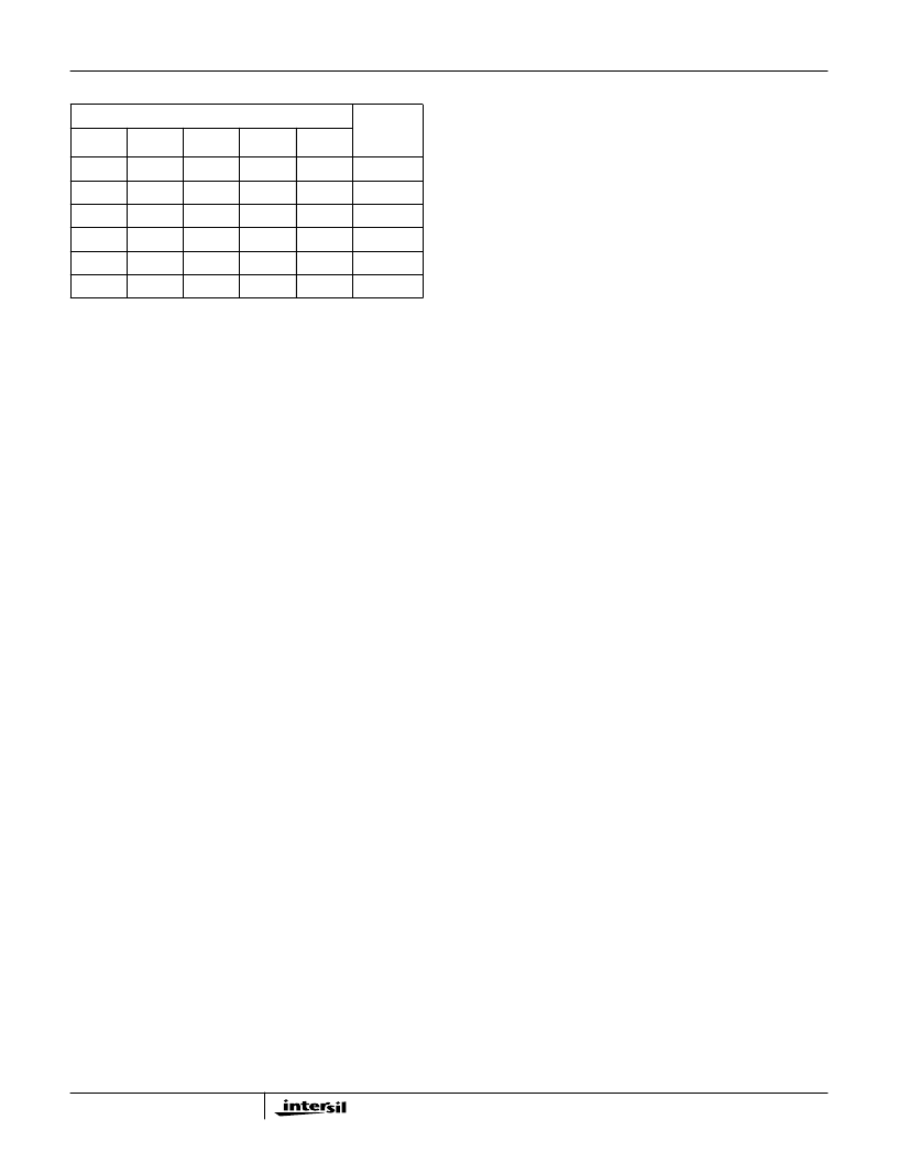
1
0
1
0
1
3.0
1
0
1
0
0
3.1
1
0
0
1
1
3.2
1
0
0
1
0
3.3
1
0
0
0
1
3.4
1
0
0
0
0
3.5
NOTE: 0 = connected to GND, 1 = open or connected to 5V through
pull-up resistors
TABLE 1. OUT1 VOLTAGE PROGRAM (Continued)
PIN NAME
NOMINAL
DACOUT
VOLTAGE
VID4
VID3
VID2
VID1
VID0
HIP6020A
相关PDF资料 |
PDF描述 |
|---|---|
| HIP6020ACB | Advanced Dual PWM and Dual Linear Power Controller |
| HIP6020EVAL1 | Advanced Dual PWM and Dual Linear Power Controller |
| HIP6020 | FPGA - 100000 SYSTEM GATE 2.5 VOLT - NOT RECOMMENDED for NEW DESIGN |
| HIP6020CB | Advanced Dual PWM and Dual Linear Power Controller |
| HIP6301VCBZ-T | 100000 SYSTEM GATE 1.8 VOLT FPGA - NOT RECOMMENDED for NEW DESIGN |
相关代理商/技术参数 |
参数描述 |
|---|---|
| HIP6020A_01 | 制造商:INTERSIL 制造商全称:Intersil Corporation 功能描述:Advanced Dual PWM and Dual Linear Power Controller |
| HIP6020ACB | 制造商:Intersil Corporation 功能描述: |
| HIP6020ACB WAF | 制造商:Harris Corporation 功能描述: |
| HIP6020ACB-T | 制造商:Rochester Electronics LLC 功能描述:DUAL PWM AND 2 LINEAR CONTROLLER W/O VID=11111 SHUTDOWN - Tape and Reel |
| HIP6020CB | 制造商:Rochester Electronics LLC 功能描述:DUAL PWM AND 2 LINEAR CONTROLLER - Bulk |
发布紧急采购,3分钟左右您将得到回复。