- 您现在的位置:买卖IC网 > PDF目录22311 > HIP6021CB (Intersil)IC REG QD BCK/LINEAR 28-SOIC PDF资料下载
参数资料
| 型号: | HIP6021CB |
| 厂商: | Intersil |
| 文件页数: | 14/15页 |
| 文件大小: | 408K |
| 描述: | IC REG QD BCK/LINEAR 28-SOIC |
| 标准包装: | 26 |
| 拓扑: | 降压(降压)同步(1),线性(LDO)(3) |
| 功能: | 任何功能 |
| 输出数: | 4 |
| 频率 - 开关: | 215kHz |
| 电压/电流 - 输出 1: | 控制器 |
| 电压/电流 - 输出 2: | 控制器 |
| 电压/电流 - 输出 3: | 控制器 |
| 带 LED 驱动器: | 无 |
| 带监控器: | 无 |
| 带序列发生器: | 无 |
| 电源电压: | 5 V ~ 12 V |
| 工作温度: | 0°C ~ 70°C |
| 安装类型: | * |
| 封装/外壳: | 28-SOIC(0.295",7.50mm 宽) |
| 供应商设备封装: | * |
| 包装: | 管件 |
14
each drive a MOSFET or a NPN bipolar as a pass transistor.
All these transistors should be selected based upon
r
DS(ON)
, current gain, saturation voltages, gate supply
requirements, and thermal management considerations.
PWM MOSFET Selection and Considerations
In high-current PWM applications, the MOSFET power
dissipation, package selection and heatsink are the
dominant design factors. The power dissipation includes two
loss components; conduction loss and switching loss. These
losses are distributed between the upper and lower
MOSFETs according to duty factor (see the equations
below). The conduction losses are the main component of
power dissipation for the lower MOSFETs. Only the upper
MOSFET has significant switching losses, since the lower
device turns on and off into near zero voltage.
The equations below assume linear voltage-current
transitions and do not model power loss due to the reverse-
recovery of the lower MOSFETs body diode. The gate-
charge losses are dissipated by the HIP6021 and don't heat
the MOSFETs. However, large gate-charge increases the
switching time, t
SW
which increases the upper MOSFET
switching losses. Ensure that both MOSFETs are within their
maximum junction temperature at high ambient temperature
by calculating the temperature rise according to package
thermal-resistance specifications. A separate heatsink may
be necessary depending upon MOSFET power, package
type, ambient temperature and air flow.
The r
DS(ON)
is different for the two equations above even if
the same device is used for both. This is because the gate
drive applied to the upper MOSFET is different than the
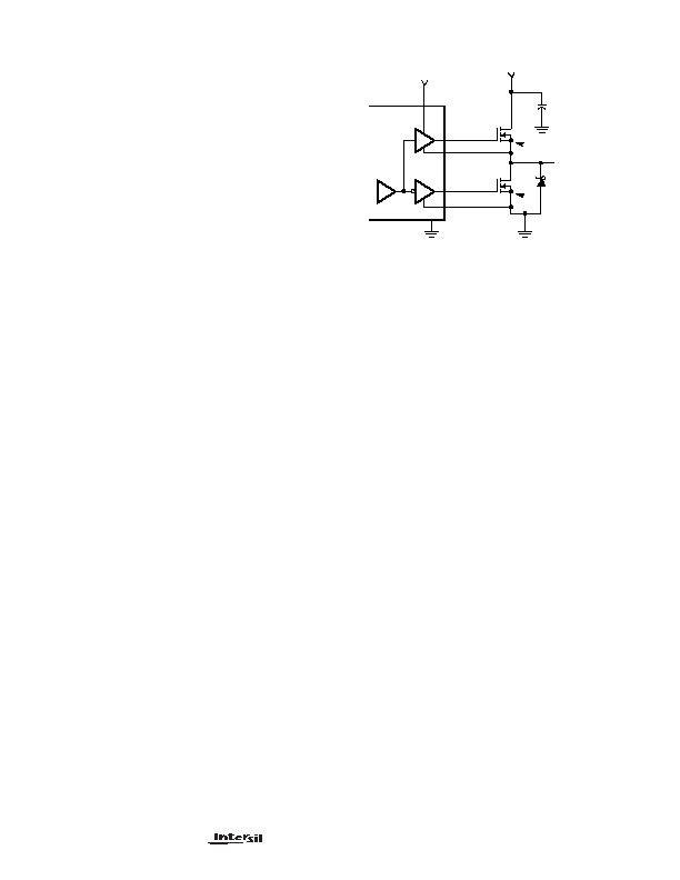
lower MOSFET. Figure 11 shows the gate drive where the
upper MOSFETs gate-to-source voltage is approximately
VCC less the input supply. For +5V main power and +12VDC
for the bias, the gate-to-source voltage of Q1 is 7V. The
lower gate drive voltage is +12VDC. A logic-level MOSFET is
a good choice for Q1 and a logic-level MOSFET can be used
for Q2 if its absolute gate-to-source voltage rating exceeds
the maximum voltage applied to VCC.
Rectifier CR1 is a clamp that catches the negative inductor
swing during the dead time between the turn off of the lower
MOSFET and the turn on of the upper MOSFET. The diode
must be a Schottky type to prevent the lossy parasitic
MOSFET body diode from conducting. It is acceptable to
omit the diode and let the body diode of the lower MOSFET
clamp the negative inductor swing, but efficiency could drop
one or two percent as a result. The diode's rated reverse
breakdown voltage must be greater than the maximum input
voltage.
Linear Controller Transistor Selection
The main criteria for selection of transistors for the linear
regulators is package selection for efficient removal of heat.
The power dissipated in a linear regulator is:
Select a package and heatsink that maintains the junction
temperature below the rating with a the maximum expected
ambient temperature.
When selecting bipolar NPN transistors for use with the
linear controllers, insure the current gain at the given
operating VCE is sufficiently large to provide the desired
output load current when the base is fed with the minimum
driver output current.
P
UPPER
I
O
2
r
DS ON
( )
?/DIV>
V
OUT
?/DIV>
V
IN
----------------------------------------------------------- -
I
O
V
IN
?/DIV>
t
SW
?/DIV>
F
S
?/DIV>
2
----------------------------------------------------
+
=
P
LOWER
I
O
2
r
DS ON
( )
?/DIV>
V
IN
V
OUT
(
)
?/DIV>
V
IN
-------------------------------------------------------------------------------- -
=
FIGURE 11. UPPER GATE DRIVE - DIRECT V
CC
DRIVE OPTION
+12V
PGND
HIP6021
GND
LGATE
UGATE
PHASE
VCC
+5V OR LESS
NOTE:
NOTE:
V
GS
H V
CC
Q1
Q2
+
-
V
GS
H V
CC
-5V
CR1
P
LINEAR
I
O
V
IN
V
OUT
(
)
?/DIV>
=
HIP6021
相关PDF资料 |
PDF描述 |
|---|---|
| GBM25DRSN | CONN EDGECARD 50POS DIP .156 SLD |
| ISL6529CR-T | IC REG DL BCK/LINEAR SYNC 16-QFN |
| V375C3V3H50B | CONVERTER MOD DC/DC 3.3V 50W |
| SE15PB-M3/85A | DIODE ESD 1.5A 100V DO-220AA |
| H7FXH-1506M | CABLE D-SUB - HFP15H/AE15M/X |
相关代理商/技术参数 |
参数描述 |
|---|---|
| HIP6021CB-T | 功能描述:IC REG QD BCK/LINEAR 28-SOIC RoHS:否 类别:集成电路 (IC) >> PMIC - 稳压器 - 线性 + 切换式 系列:- 标准包装:2,500 系列:- 拓扑:降压(降压)同步(3),线性(LDO)(2) 功能:任何功能 输出数:5 频率 - 开关:300kHz 电压/电流 - 输出 1:控制器 电压/电流 - 输出 2:控制器 电压/电流 - 输出 3:控制器 带 LED 驱动器:无 带监控器:无 带序列发生器:是 电源电压:5.6 V ~ 24 V 工作温度:-40°C ~ 85°C 安装类型:* 封装/外壳:* 供应商设备封装:* 包装:* |
| HIP6021CBZ | 功能描述:电压模式 PWM 控制器 SINGLE PWM & TRPL LINEAR CNTRLR RoHS:否 制造商:Texas Instruments 输出端数量:1 拓扑结构:Buck 输出电压:34 V 输出电流: 开关频率: 工作电源电压:4.5 V to 5.5 V 电源电流:600 uA 最大工作温度:+ 125 C 最小工作温度:- 40 C 封装 / 箱体:WSON-8 封装:Reel |
| HIP6021CBZ-T | 功能描述:电压模式 PWM 控制器 SINGLE PWM & TRPL LINEAR CNTRLR RoHS:否 制造商:Texas Instruments 输出端数量:1 拓扑结构:Buck 输出电压:34 V 输出电流: 开关频率: 工作电源电压:4.5 V to 5.5 V 电源电流:600 uA 最大工作温度:+ 125 C 最小工作温度:- 40 C 封装 / 箱体:WSON-8 封装:Reel |
| HIP6021EVAL1 | 功能描述:电源管理IC开发工具 HIP6021 EVAL BRD RoHS:否 制造商:Maxim Integrated 产品:Evaluation Kits 类型:Battery Management 工具用于评估:MAX17710GB 输入电压: 输出电压:1.8 V |
| HIP6028 | 制造商:INTERSIL 制造商全称:Intersil Corporation 功能描述:Advanced PWM and Dual Linear Power Control with Integrated ACPI Support Interface |
发布紧急采购,3分钟左右您将得到回复。