- 您现在的位置:买卖IC网 > PDF目录22311 > HIP6521CB (Intersil)IC REG QD BCK/LINEAR SYNC 16SOIC PDF资料下载
参数资料
| 型号: | HIP6521CB |
| 厂商: | Intersil |
| 文件页数: | 7/13页 |
| 文件大小: | 356K |
| 描述: | IC REG QD BCK/LINEAR SYNC 16SOIC |
| 标准包装: | 48 |
| 拓扑: | 降压(降压)同步(1),线性(LDO)(3) |
| 功能: | 任何功能 |
| 输出数: | 4 |
| 频率 - 开关: | 300kHz |
| 电压/电流 - 输出 1: | 控制器 |
| 电压/电流 - 输出 2: | 控制器 |
| 电压/电流 - 输出 3: | 控制器 |
| 带 LED 驱动器: | 无 |
| 带监控器: | 无 |
| 带序列发生器: | 无 |
| 电源电压: | 4.75 V ~ 5.25 V |
| 工作温度: | 0°C ~ 70°C |
| 安装类型: | * |
| 封装/外壳: | 16-SOIC(0.154",3.90mm 宽) |
| 供应商设备封装: | * |
| 包装: | 管件 |
7
FN4837.5
October 16, 2006
1. The maximum r
DS(ON)
at the highest junction temperature.
2. The minimum I
OCSET
from the specification table.
3. Determine I
PEAK
for I
PEAK
> I
OUT(MAX)
+ (I)/2, where
I is the output inductor ripple current.
For an equation for the ripple current see the section under
component guidelines titled Output Inductor Selection.
Output Voltage Selection
The output voltage of the PWM converter can be
resistor-programmed to any level between V
IN
and 0.8V.
However, since the value of R
S1
is affecting the values of
the rest of the compensation components, it is advisable its
value is kept between 2k& and 5k&.
All linear regulators output voltages are set by means of
external resistor dividers as shown in Figure 4. The two
resistors used to set the voltage on each of the three linear
regulators have to meet the following criteria: their value
while in a parallel connection has to be less than 5k&, or
otherwise said, the following relationship has to be met:
There may be a second restriction on the size of the
resistors used to set the linear regulators output voltage
based on ACPI functionality. Read the ACPI
Implementation section under Application Guidelines to
see if this additional constraint concerns your application. To
ensure the parallel combination of the feedback resistors
equals a certain chosen value, R
FB
, use the following
equations:
, where
V
OUT
- the desired output voltage,
V
FB
- feedback (reference) voltage, 0.8V.
Application Guidelines
Soft-Start Interval
The soft-start function controls the output voltages rate of rise
to limit the current surge at start-up. The soft-start function is
integrated on the chip and the soft-start interval is thus fixed.
Layout Considerations
MOSFETs switch very fast and efficiently. The speed with
which the current transitions from one device to another
causes voltage spikes across the interconnecting
impedances and parasitic circuit elements. The voltage
spikes can degrade efficiency, radiate noise into the circuit,
and lead to device overvoltage stress. Careful component
layout and printed circuit design minimizes the voltage
spikes in the converter. Consider, as an example, the
turn-off transition of the upper PWM MOSFET. Prior to
turn-off, the upper MOSFET was carrying the full load
current. During the turn-off, current stops flowing in the
upper MOSFET and is picked up by the lower MOSFET or
Schottky diode. Any inductance in the switched current
path generates a large voltage spike during the switching
interval. Careful component selection, tight layout of the
critical components, and short, wide circuit traces minimize
the magnitude of voltage spikes. See the Application Note
AN9908 for evaluation board drawings of the component
placement and printed circuit board.
There are two sets of critical components in a DC/DC
converter using a HIP6521 controller. The switching power
components are the most critical because they switch large
amounts of energy, and as such, they tend to generate
UGATE
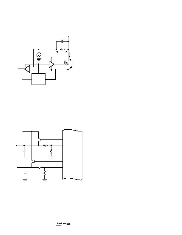
OCSET
PHASE
OCC
+
-
GATE
CONTROL
VCC
OC
40?/SPAN>A
V
DS(ON)
i
D
V
SET
R
OCSET
V
IN
= +5V
OVERCURRENT TRIP:
I
OCSET
+
+
FIGURE 3. OVERCURRENT DETECTION
PWM
DRIVE
i
D
r
DS ON
( )
?/DIV>
I
OCSET
R
OCSET
?/DIV>
>
V
DS
V
SET
>
V
PHASE
V
IN
V
DS
=
V
OCSET
V
IN
V
SET
=
DRIVE3
FB3
FB4
C
OUT4
C
OUT3
Q4
HIP6521
V
OUT3
V
OUT4
Q5
+3.3V
IN
DRIVE4
R
S3
R
P3
R
S4
R
P4
V
OUT
0.8 1
R
S
R
P
------- -
+
?/DIV>
?/DIV>
?/DIV>
?/DIV>
?/DIV>
?/DIV>
?/DIV>
=
FIGURE 4. ADJUSTING THE OUTPUT VOLTAGE OF ANY OF
THE FOUR REGULATORS (OUTPUTS 3 AND 4
PICTURED)
+
+
R
S
R
P
?/DIV>
R
S
R
P
+
--------------------- - 5k&
<
R
S
V
OUT
V
FB
--------------- - R
FB
?/DIV>
=
R
P
R
S
V
FB
?/DIV>
V
OUT
V
FB
-------------------------------- -
=
HIP6521
相关PDF资料 |
PDF描述 |
|---|---|
| HIP6021CB | IC REG QD BCK/LINEAR 28-SOIC |
| GBM25DRSN | CONN EDGECARD 50POS DIP .156 SLD |
| ISL6529CR-T | IC REG DL BCK/LINEAR SYNC 16-QFN |
| V375C3V3H50B | CONVERTER MOD DC/DC 3.3V 50W |
| SE15PB-M3/85A | DIODE ESD 1.5A 100V DO-220AA |
相关代理商/技术参数 |
参数描述 |
|---|---|
| HIP6521CB-T | 功能描述:IC REG QD BCK/LINEAR SYNC 16SOIC RoHS:否 类别:集成电路 (IC) >> PMIC - 稳压器 - 线性 + 切换式 系列:- 标准包装:2,500 系列:- 拓扑:降压(降压)同步(3),线性(LDO)(2) 功能:任何功能 输出数:5 频率 - 开关:300kHz 电压/电流 - 输出 1:控制器 电压/电流 - 输出 2:控制器 电压/电流 - 输出 3:控制器 带 LED 驱动器:无 带监控器:无 带序列发生器:是 电源电压:5.6 V ~ 24 V 工作温度:-40°C ~ 85°C 安装类型:* 封装/外壳:* 供应商设备封装:* 包装:* |
| HIP6521CBZ | 功能描述:电压模式 PWM 控制器 4 IN 1 PWM/LINEAR CNTRLR 5V RoHS:否 制造商:Texas Instruments 输出端数量:1 拓扑结构:Buck 输出电压:34 V 输出电流: 开关频率: 工作电源电压:4.5 V to 5.5 V 电源电流:600 uA 最大工作温度:+ 125 C 最小工作温度:- 40 C 封装 / 箱体:WSON-8 封装:Reel |
| HIP6521CBZA | 功能描述:IC REG QD BCK/LINEAR 16-SOIC RoHS:是 类别:集成电路 (IC) >> PMIC - 稳压器 - 线性 + 切换式 系列:- 标准包装:2,500 系列:- 拓扑:降压(降压)同步(3),线性(LDO)(2) 功能:任何功能 输出数:5 频率 - 开关:300kHz 电压/电流 - 输出 1:控制器 电压/电流 - 输出 2:控制器 电压/电流 - 输出 3:控制器 带 LED 驱动器:无 带监控器:无 带序列发生器:是 电源电压:5.6 V ~ 24 V 工作温度:-40°C ~ 85°C 安装类型:* 封装/外壳:* 供应商设备封装:* 包装:* |
| HIP6521CBZA-T | 功能描述:IC REG QD BCK/LINEAR 16-SOIC RoHS:是 类别:集成电路 (IC) >> PMIC - 稳压器 - 线性 + 切换式 系列:- 标准包装:2,500 系列:- 拓扑:降压(降压)同步(3),线性(LDO)(2) 功能:任何功能 输出数:5 频率 - 开关:300kHz 电压/电流 - 输出 1:控制器 电压/电流 - 输出 2:控制器 电压/电流 - 输出 3:控制器 带 LED 驱动器:无 带监控器:无 带序列发生器:是 电源电压:5.6 V ~ 24 V 工作温度:-40°C ~ 85°C 安装类型:* 封装/外壳:* 供应商设备封装:* 包装:* |
| HIP6521CBZ-T | 功能描述:电压模式 PWM 控制器 4 IN 1 PWM/LINEAR CNTRLR 5V RoHS:否 制造商:Texas Instruments 输出端数量:1 拓扑结构:Buck 输出电压:34 V 输出电流: 开关频率: 工作电源电压:4.5 V to 5.5 V 电源电流:600 uA 最大工作温度:+ 125 C 最小工作温度:- 40 C 封装 / 箱体:WSON-8 封装:Reel |
发布紧急采购,3分钟左右您将得到回复。