- 您现在的位置:买卖IC网 > PDF目录1996 > HMC704LP4E (Hittite Microwave Corporation)IC FRACT-N PLL 16BIT 24QFN PDF资料下载
参数资料
| 型号: | HMC704LP4E |
| 厂商: | Hittite Microwave Corporation |
| 文件页数: | 10/44页 |
| 文件大小: | 0K |
| 描述: | IC FRACT-N PLL 16BIT 24QFN |
| 标准包装: | 1 |
| 类型: | 整数 N/小数 N 分频 |
| PLL: | 是 |
| 输入: | CMOS |
| 输出: | CMOS |
| 电路数: | 1 |
| 比率 - 输入:输出: | 1:1 |
| 差分 - 输入:输出: | 是/无 |
| 频率 - 最大: | 8GHz |
| 除法器/乘法器: | 是/无 |
| 电源电压: | 3.3V,5V |
| 工作温度: | -40°C ~ 85°C |
| 安装类型: | 表面贴装 |
| 封装/外壳: | 24-VQFN 裸露焊盘 |
| 供应商设备封装: | 24-QFN 裸露焊盘(4x4) |
| 包装: | 标准包装 |
| 其它名称: | 1127-1066-6 |
第1页第2页第3页第4页第5页第6页第7页第8页第9页当前第10页第11页第12页第13页第14页第15页第16页第17页第18页第19页第20页第21页第22页第23页第24页第25页第26页第27页第28页第29页第30页第31页第32页第33页第34页第35页第36页第37页第38页第39页第40页第41页第42页第43页第44页
p
ll
s
-
s
M
T
5 - 18
HMC704LP4E
v03.1211
8 GHz fractionaL-n PLL
For price, delivery, and to place orders: Hittite Microwave Corporation,20 Alpha Road, Chelmsford, MA 01824
Phone: 978-250-3343
Fax: 978-250-3373
Order On-line at www.hittite.com
Application Support: Phone: 978-250-3343 or apps@hittite.com
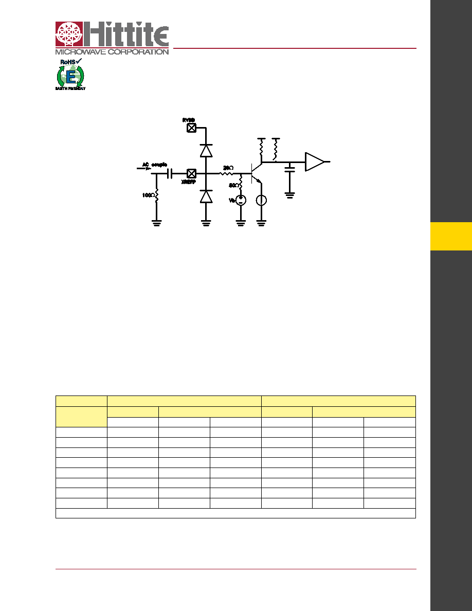
reference input Stage
The reference buffer provides the path from an external reference source (generally crystal based) to the R divider, and
eventually to the phase detector. The buffer has two modes of operation. High Gain (recommended below 200MHz),
and High frequency, for 200 to 350MHz operation. The buffer is internally DC biased, with 100 Ohm internal termina-
tion. For 50 Ohm match, an external 100 Ohm resistance to ground should be added, followed by an AC coupling ca-
pacitance (impedance < 1 Ohm), then to the XREFP pin of the part.
At low frequencies, a relatively square reference is recommended to keep the input slew rate high. At higher frequen-
cies, a square or sinusoid can be used. The following table shows the recommended operating regions for different
reference frequencies. If operating outside these regions the part will normally still operate, but with degraded perfor-
mance.
Minimum pulse width at the reference buffer input is 2.5ns. For best spur performance when R = 1, the pulse width
should be (2.5ns + 8Tps), where Tps is the period of the VCO at the prescaler input. When R > 1 minimum pulse width
is 2.5ns.
table 6. reference Sensitivity table
square Input
sinusoidal Input
Frequency
(MHz)
slew > 0.5V/ns
Recommended swing (Vpp)
Recommended Power Range (dBm)
Recommended
Min
Max
Recommended
Min
Max
< 10
YEs
0.6
2.5
x
10
YEs
0.6
2.5
x
25
YEs
0.6
2.5
ok
8
15
50
YEs
0.6
2.5
YEs
6
15
100
YEs
0.6
2.5
YEs
5
15
150
ok
0.9
2.5
YEs
4
12
200
ok
1.2
2.5
YEs
3
8
200 to 350
x
YEs1
5
10
Note: For greater than 200MHz operation, use buffer in High Frequency Mode. Reg[8] bit 21 = 1
Input referred phase noise of the PLL when operating at 50MHz is between -150 and -156dBc/Hz at 10kHz offset de-
pending upon the mode of operation. The input reference signal should be 10dB better than this floor to avoid deg-
radation of the PLL noise contribution. It should be noted that such low levels are only necessary if the PLL is the domi-
nant noise contributor and these levels are required for the system goals.
Figure 27. Reference Path Input Stage
相关PDF资料 |
PDF描述 |
|---|---|
| HMC830LP6GE | IC FRACT-N PLL W/VCO 40QFN |
| HMP8117CNZ | IC VIDEO DECODER NTSC/PAL 80PQFP |
| HMP8156ACNZ | IC VIDEO ENCODER NTSC/PAL 64MQFP |
| HSP45102SC-40Z | IC OSC NCO 40MHZ 28-SOIC |
| HSP45106JC-33Z | IC OSC NCO 33MHZ 84-PLCC |
相关代理商/技术参数 |
参数描述 |
|---|---|
| HMC704LP4ETR | 制造商:Hittite Microwave Corp 功能描述:IC FRACT-N PLL 16BIT 24QFN |
| HMC705LP4 | 制造商:HITTITE 制造商全称:Hittite Microwave Corporation 功能描述:6.5 GHz PROGRAMMABLE DIVIDER (N = 1 - 17) |
| HMC705LP4E | 制造商:Hittite Microwave Corp 功能描述:IC DIVIDER HBT PROGR 24-QFN |
| HMC705LP4ETR | 功能描述:IC DIVIDER HBT PROGR 24QFN 制造商:analog devices inc. 系列:- 包装:剪切带(CT) 零件状态:在售 功能:分频器 频率:100MHz ~ 6.5GHz RF 类型:- 辅助属性:- 封装/外壳:24-VFQFN 裸露焊盘 供应商器件封装:24-QFN(4x4) 标准包装:1 |
| hmc706lc3c | 制造商:Hittite Microwave Corp 功能描述:IC CONV NRZ-RZ 13GBPS 16SMD |
发布紧急采购,3分钟左右您将得到回复。