参数资料
| 型号: | HSP45102SC-40Z |
| 厂商: | Intersil |
| 文件页数: | 4/9页 |
| 文件大小: | 0K |
| 描述: | IC OSC NCO 40MHZ 28-SOIC |
| 标准包装: | 26 |
| 类型: | 数控振荡器(NCO) |
| 频率: | 40MHz |
| 电源电压: | 4.75 V ~ 5.25 V |
| 电流 - 电源: | 99mA |
| 工作温度: | 0°C ~ 70°C |
| 封装/外壳: | 28-SOIC(0.295",7.50mm 宽) |
| 包装: | 管件 |
| 供应商设备封装: | 28-SOIC W |
| 安装类型: | 表面贴装 |
4
FN2810.9
April 25, 2007
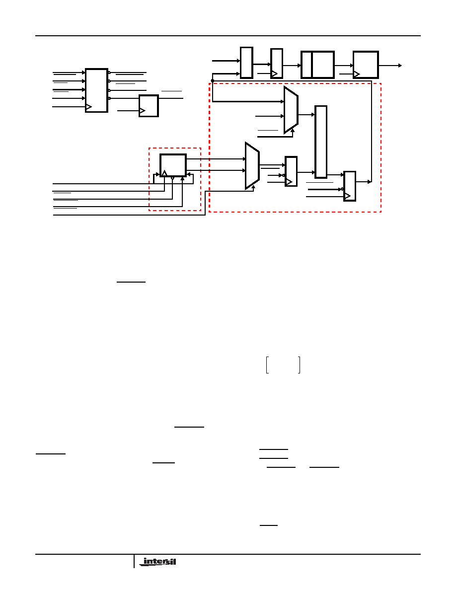
Functional Description
The NCO12 produces a 12-bit sinusoid whose frequency
and phase are digitally controlled. The frequency of the sine
wave is determined by one of two 32-bit words. Selection of
the active word is made by SEL_L/M. The phase of the
output is controlled by the two-bit input P0-1, which is used
to select a phase offset of 0°, 90°, 180°, or 270°.
As shown in the Block Diagram, the NCO12 consists of a
Frequency Control Section, a Phase Accumulator, a Phase
Offset Adder and a Sine ROM. The Frequency Control
section serially loads the frequency control word into the
frequency register. The Phase Accumulator and Phase
Offset Adder compute the phase angle using the frequency
control word and the two phase modulation inputs. The Sine
ROM generates the sine of the computed phase angle. The
format of the 12-bit output is offset binary.
Frequency Control Section
The Frequency Control Section shown in Figure 1 serially
loads the frequency data into a 64-bit, bidirectional shift
register. The shift direction is selected with the MSB/LSB
input. When this input is high, the frequency control word on
the SD input is shifted into the register MSB first. When
MSB/LSB is low the data is shifted in LSB first. The register
shifts on the rising edge of SCLK when SFTEN is low. The
The 64 bits of the frequency register are sent to the Phase
Accumulator Section where 32 bits are selected to control
the frequency of the sinusoidal output.
Phase Accumulator Section
The phase accumulator and phase offset adder compute the
phase of the sine wave from the frequency control word and
the phase modulation bits P0-1. The architecture is shown in
Figure 1. The most significant 13 bits of the 32-bit phase
accumulator are summed with the two-bit phase offset to
generate the 13-bit phase input to the Sine Rom. A value of
0 corresponds to 0°, a value of 1000 hexadecimal
corresponds to a value of 180°.
The phase accumulator advances the phase by the amount
programmed into the frequency control register. The output
frequency is equal to:
where N is the 32 bits of frequency control word that is
programmed. INT[] is the integer of the computation. For
example, if the control word is 20000000 hexadecimal and the
clock frequency is 30MHz, then the output frequency would
be fCLK/8, or 3.75MHz.
The frequency control multiplexer selects the least
significant 32 bits from the 64-bit frequency control register
when SEL_L/M is high, and the most significant 32 bits
when SEL_L/M is low. When only one frequency word is
desired, SEL_L/M and MSB/LSB must be either both high or
both low. This is due to the fact that when a frequency
control word is loaded into the shift register LSB first, it
enters through the most significant bit of the register. After
32 bits have been shifted in, they will reside in the 32 most
significant bits of the 64-bit register.
When TXFR is asserted, the 32 bits selected by the frequency
control multiplexer are clocked into the phase accumulator
/
13 MSBs
R.P0-1
CLK
P0-1
CLK
/ 32
R
E
G
R
E
G
/ 32
ACCUMULATOR
INPUT
REGISTER
A
D
E
R
R.TXFR
/ 32
CLK
/
32
‘0’
/ 32
64-BIT
SHIFT
REG
/
32
/
32
PHASE ACCUMULATOR
2-DLY
R
E
G
R
E
G
R.P0-1
PHASE OFFSET ADDER
/
13
A
D
E
R
/
13
R
E
G
SINE
ROM
/
12
CLK
FRCTRL
SD
SCLK
FREQUENCY
CONTROL
SECTION
R.LOAD
SFTEN
MSB/LSB
R.ENPHAC
R.TXFR
R.LOAD
TXFR
LOAD
SEL_L/M
R.ENPHAC
0-31
32-63
(HIGH SELECTS FRCTRL0-31, LOW SELECTS FRCTRL32-63)
OUT0-11
4-DLY
R
E
G
ENPHAC
FIGURE 1. NCO-12 FUNCTIONAL BLOCK DIAGRAM
R
E
G
CLK
0
1
MU
X
0
1
MU
X
f
LO
Nf
CLK
×
2
32
(), or
=
(EQ. 1)
N
INT
f
OUT
f
CLK
-------------
2
32
,
=
(EQ. 2)
HSP45102
相关PDF资料 |
PDF描述 |
|---|---|
| HSP45106JC-33Z | IC OSC NCO 33MHZ 84-PLCC |
| HSP45116AVC-52Z | IC OSC NCO 52MHZ 160-MQFP |
| ICL7109EPL+ | IC ADC 12BIT 3-ST 40-DIP |
| ICM7217AIPI | IC OSC UP/DWN CNTR 2MHZ 28-DIP |
| ICM7217CIPI | IC OSC UP/DWN CNTR 2MHZ 28-DIP |
相关代理商/技术参数 |
参数描述 |
|---|---|
| HSP45102SI-33 | 制造商:Rochester Electronics LLC 功能描述:12 BIT NUMERICALLY CONTROLLED OSCILLATOR - Bulk |
| HSP45102SI-3396 | 功能描述:可编程振荡器 12 BIT NCO 28LD SOIC,T&R,33MHZ,IND RoHS:否 制造商:IDT 封装 / 箱体:5 mm x 7 mm x 1.5 mm 频率:15.476 MHz to 866.67, 975 MHz to 1300 MHz 频率稳定性:+/- 50 PPM 电源电压:3.63 V 负载电容:10 pF 端接类型:SMD/SMT 输出格式:LVPECL 最小工作温度:- 40 C 最大工作温度:+ 85 C 尺寸:7 mm W x 5 mm L x 1.5 mm H 封装: |
| HSP45102SI-33Z | 功能描述:可编程振荡器 W/ANNEAL 12 BIT NCO 28 33MHZ IND RoHS:否 制造商:IDT 封装 / 箱体:5 mm x 7 mm x 1.5 mm 频率:15.476 MHz to 866.67, 975 MHz to 1300 MHz 频率稳定性:+/- 50 PPM 电源电压:3.63 V 负载电容:10 pF 端接类型:SMD/SMT 输出格式:LVPECL 最小工作温度:- 40 C 最大工作温度:+ 85 C 尺寸:7 mm W x 5 mm L x 1.5 mm H 封装: |
| HSP45102SI-40 | 制造商:Rochester Electronics LLC 功能描述:- Bulk |
| HSP45106 | 制造商:INTERSIL 制造商全称:Intersil Corporation 功能描述:16-Bit Numerically Controlled Oscillator |
发布紧急采购,3分钟左右您将得到回复。