- 您现在的位置:买卖IC网 > PDF目录384468 > HY5PS1G421LM (Hynix Semiconductor Inc.) 1Gb DDR2 SDRAM(DDP) PDF资料下载
参数资料
| 型号: | HY5PS1G421LM |
| 厂商: | Hynix Semiconductor Inc. |
| 英文描述: | 1Gb DDR2 SDRAM(DDP) |
| 中文描述: | 1G DDR2内存(铂) |
| 文件页数: | 14/79页 |
| 文件大小: | 1109K |
| 代理商: | HY5PS1G421LM |
第1页第2页第3页第4页第5页第6页第7页第8页第9页第10页第11页第12页第13页当前第14页第15页第16页第17页第18页第19页第20页第21页第22页第23页第24页第25页第26页第27页第28页第29页第30页第31页第32页第33页第34页第35页第36页第37页第38页第39页第40页第41页第42页第43页第44页第45页第46页第47页第48页第49页第50页第51页第52页第53页第54页第55页第56页第57页第58页第59页第60页第61页第62页第63页第64页第65页第66页第67页第68页第69页第70页第71页第72页第73页第74页第75页第76页第77页第78页第79页
Rev. 0.2 / Oct. 2005
14
1
HY5PS12421(L)M
HY5PS12821(L)M
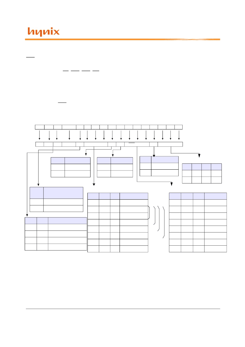
2.3.2.1 DDR2 SDRAM Mode Register Set (MRS)
The mode register stores the data for controlling the various operating modes of DDR2 SDRAM. It controls
CAS latency, burst length, burst sequence, test mode, DLL reset, tWR and various vendor specific options to
make DDR2 SDRAM useful for various applications. The default value of the mode register is not defined,
therefore the mode register must be written after power-up for proper operation. The mode register is written
by asserting low on CS, RAS, CAS, WE, BA0 and BA1, while controlling the state of address pins A0 ~ A15.
The DDR2 SDRAM should be in all bank precharge with CKE already high prior to writing into the mode reg-
ister. The mode register set command cycle time (tMRD) is required to complete the write operation to the
mode register. The mode register contents can be changed using the same command and clock cycle
requirements during normal operation as long as all banks are in the precharge state. The mode register is
divided into various fields depending on functionality. Burst length is defined by A0 ~ A2 with options of 4 and
8 bit burst lengths. The burst length decodes are compatible with DDR SDRAM. Burst address sequence type
is defined by A3, CAS latency is defined by A4 ~ A6. The DDR2 doesn’t support half clock latency mode. A7
is used for test mode. A8 is used for DLL reset. A7 must be set to low for normal MRS operation. Write recov-
ery time tWR is defined by A9 ~ A11. Refer to the table for specific codes.
Address Field
CAS Latency
A
6
0
0
0
0
1
1
1
1
A
5
0
0
1
1
0
0
1
1
A
4
0
1
0
1
0
1
0
1
Latency
Reserved
Reserved
2(optional)
3
4
5
6
Reserved
A
7
0
1
mode
Normal
Test
A
3
0
1
Burst Type
Sequential
Interleave
A
8
0
1
DLL Reset
No
Yes
Mode Register
BA
1
BA
0
A
11
A
10
A
9
A
8
A
7
A
6
A
5
A
4
A
3
A
2
A
1
A
0
0
TM
CAS Latency
BT
DLL
0*
1
WR
Write recovery for autoprecharge
A
11
0
0
0
0
1
1
1
1
A
10
0
0
1
1
0
0
1
1
A
9
0
1
0
1
0
1
0
1
WR(cycles)
Reserved
2
3
4
5
6
Reserved
Reserved
A
15
~ A
13
0
Burst Length
Burst Length
A
2
0
0
A
1
1
1
A
0
0
1
BL
4
8
*1 : BA2 and A13~A15 are reserved for future use and must be programmed to 0 when setting the mode register.
* 2: WR(write recovery for autoprecharge) min is determined by tCK max and WR max is determined by tCK min.
WR in clock cycles is calculated by dividing tWR (in ns) by tCK (in ns) and rounding up to the next integer
(WR[cycles] = tWR(ns)/tCK(ns)). The mode register must be programmed to this value. This is also used with
tRP to determine tDAL.
BA
2
0*
1
BA1
0
0
1
1
BA0
0
1
0
1
MRS mode
MRS
EMRS(1)
EMRS(2): Reserved
EMRS(3): Reserved
D
D
D
D
*2
A
12
PD
A
12
Active power
down exit time
Fast exit(use t
XARD
)
Slow exit(use t
XARDS
)
0
1
相关PDF资料 |
PDF描述 |
|---|---|
| HY5PS1G421LM-C4 | 1Gb DDR2 SDRAM(DDP) |
| HY5PS1G421LM-E3 | 1Gb DDR2 SDRAM(DDP) |
| HY5PS1G421M | 1Gb DDR2 SDRAM(DDP) |
| HY5PS1G421M-C4 | 1Gb DDR2 SDRAM(DDP) |
| HY5PS1G421M-E3 | 1Gb DDR2 SDRAM(DDP) |
相关代理商/技术参数 |
参数描述 |
|---|---|
| HY5PS1G421LM-C4 | 制造商:HYNIX 制造商全称:Hynix Semiconductor 功能描述:1Gb DDR2 SDRAM(DDP) |
| HY5PS1G421LM-E3 | 制造商:HYNIX 制造商全称:Hynix Semiconductor 功能描述:1Gb DDR2 SDRAM(DDP) |
| HY5PS1G421M | 制造商:HYNIX 制造商全称:Hynix Semiconductor 功能描述:1Gb DDR2 SDRAM(DDP) |
| HY5PS1G421M-C4 | 制造商:HYNIX 制造商全称:Hynix Semiconductor 功能描述:1Gb DDR2 SDRAM(DDP) |
| HY5PS1G421M-E3 | 制造商:HYNIX 制造商全称:Hynix Semiconductor 功能描述:1Gb DDR2 SDRAM(DDP) |
发布紧急采购,3分钟左右您将得到回复。