- 您现在的位置:买卖IC网 > PDF目录384468 > HY5PS1G831CLFP-E3 (HYNIX SEMICONDUCTOR INC) 1Gb DDR2 SDRAM PDF资料下载
参数资料
| 型号: | HY5PS1G831CLFP-E3 |
| 厂商: | HYNIX SEMICONDUCTOR INC |
| 元件分类: | DRAM |
| 英文描述: | 1Gb DDR2 SDRAM |
| 中文描述: | 128M X 8 DDR DRAM, 0.6 ns, PBGA60 |
| 封装: | ROHS COMPLIANT, FBGA-60 |
| 文件页数: | 23/37页 |
| 文件大小: | 539K |
| 代理商: | HY5PS1G831CLFP-E3 |
第1页第2页第3页第4页第5页第6页第7页第8页第9页第10页第11页第12页第13页第14页第15页第16页第17页第18页第19页第20页第21页第22页当前第23页第24页第25页第26页第27页第28页第29页第30页第31页第32页第33页第34页第35页第36页第37页
Rev. 0.2 / Dec 2006
23
HY5PS1G431C(L)FP
HY5PS1G831C(L)FP
HY5PS1G1631C(L)FP
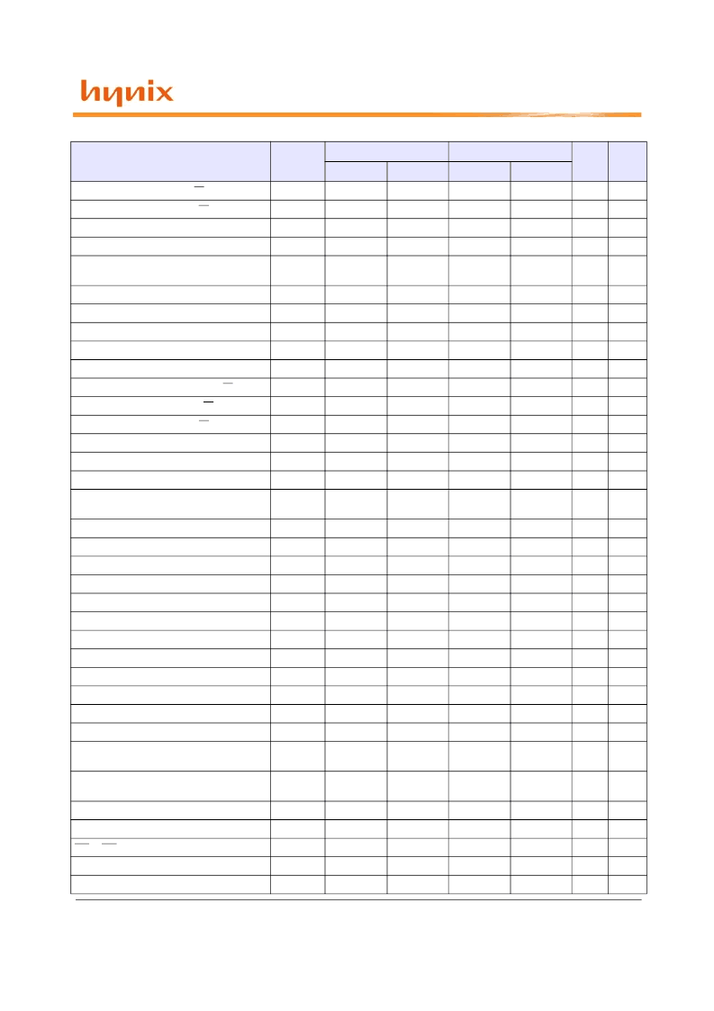
Parameter
Symbol
DDR2-667
DDR2-800
Unit
Note
min
max
min
max
DQ output access time from CK/CK
tAC
-450
+450
-400
+400
ps
DQS output access time from CK/CK
tDQSCK
-400
+400
-350
+350
ps
CK high-level width
tCH
0.45
0.55
0.45
0.55
tCK
CK low-level width
tCL
0.45
0.55
0.45
0.55
tCK
CK half period
tHP
min(tCL,
tCH)
-
min(tCL,
tCH)
-
ps
11,12
Clock cycle time, CL=x
tCK
3000
8000
2500
ps
15
DQ and DM input setup time
tDS(base)
100
-
50
-
ps
6,7,8,20
DQ and DM input hold time
tDH(base)
175
-
125
-
ps
6,7,8,21
Control & Address input pulse width for each input
tIPW
0.6
-
0.6
-
tCK
DQ and DM input pulse width for each input
tDIPW
0.35
-
0.35
-
tCK
Data-out high-impedance time from CK/CK
tHZ
-
tAC max
-
tAC max
ps
18
DQS low-impedance time from CK/CK
tLZ(DQS)
tAC min
tAC max
tAC min
tAC max
ps
18
DQ low-impedance time from CK/CK
tLZ(DQ)
2*tAC min
tAC max
2*tAC min
tAC max
ps
18
DQS-DQ skew for DQS and associated DQ signals
tDQSQ
-
240
-
200
ps
13
DQ hold skew factor
tQHS
-
340
-
300
ps
12
DQ/DQS output hold time from DQS
tQH
tHP - tQHS
-
tHP - tQHS
-
ps
First DQS latching transition to associated clock
edge
tDQSS
- 0.25
+ 0.25
- 0.25
+ 0.25
tCK
DQS input high pulse width
tDQSH
0.35
-
0.35
-
tCK
DQS input low pulse width
tDQSL
0.35
-
0.35
-
tCK
DQS falling edge to CK setup time
tDSS
0.2
-
0.2
-
tCK
DQS falling edge hold time from CK
tDSH
0.2
-
0.2
-
tCK
Mode register set command cycle time
tMRD
2
-
2
-
tCK
Write postamble
tWPST
0.4
0.6
0.4
0.6
tCK
10
Write preamble
tWPRE
0.35
-
0.35
-
tCK
Address and control input setup time
tIS(base)
200
-
175
-
ps
5,7,9,22
Address and control input hold time
tIH(base)
275
-
250
-
ps
5,7,9,23
Read preamble
tRPRE
0.9
1.1
0.9
1.1
tCK
19
Read postamble
tRPST
0.4
0.6
0.4
0.6
tCK
19
Activate to precharge command
tRAS
45
70000
45
70000
ns
3
Active to active command period for 1KB page size
products (x4, x8)
tRRD
7.5
-
7.5
-
ns
4
Active to active command period for 2KB page size
products (x16)
tRRD
10
-
10
-
ns
4
Four Active Window for 1KB page size products
tFAW
37.5
-
37.5
-
ns
Four Active Window for 2KB page size products
tFAW
50
-
50
-
ns
CAS to CAS command delay
tCCD
2
2
tCK
Write recovery time
tWR
15
-
15
-
ns
Auto precharge write recovery + precharge time
tDAL
WR+tRP
-
WR+tRP
-
tCK
14
相关PDF资料 |
PDF描述 |
|---|---|
| HY5PS1G831CLFP-S5 | 1Gb DDR2 SDRAM |
| HY5PS1G831CLFP-Y5 | 1Gb DDR2 SDRAM |
| HY5PS1G821LM-E3 | 1Gb DDR2 SDRAM(DDP) |
| HY5PS1G821M | 1Gb DDR2 SDRAM(DDP) |
| HY5PS1G821M-C4 | 1Gb DDR2 SDRAM(DDP) |
相关代理商/技术参数 |
参数描述 |
|---|---|
| HY5PS1G831CLFP-S5 | 制造商:HYNIX 制造商全称:Hynix Semiconductor 功能描述:1Gb DDR2 SDRAM |
| HY5PS1G831CLFP-Y5 | 制造商:HYNIX 制造商全称:Hynix Semiconductor 功能描述:1Gb DDR2 SDRAM |
| HY5PS1G831F | 制造商:HYNIX 制造商全称:Hynix Semiconductor 功能描述:1Gb DDR2 SDRAM |
| HY5PS1G831F-C4 | 制造商:HYNIX 制造商全称:Hynix Semiconductor 功能描述:1Gb DDR2 SDRAM |
| HY5PS1G831F-C5 | 制造商:HYNIX 制造商全称:Hynix Semiconductor 功能描述:1Gb DDR2 SDRAM |
发布紧急采购,3分钟左右您将得到回复。