- 您现在的位置:买卖IC网 > PDF目录67682 > IBM25NPE405L-3FA200CZ 32-BIT, 200 MHz, RISC PROCESSOR, PBGA324 PDF资料下载
参数资料
| 型号: | IBM25NPE405L-3FA200CZ |
| 元件分类: | 微控制器/微处理器 |
| 英文描述: | 32-BIT, 200 MHz, RISC PROCESSOR, PBGA324 |
| 封装: | 23 X 23 MM, PLASTIC, EBGA-324 |
| 文件页数: | 27/52页 |
| 文件大小: | 907K |
| 代理商: | IBM25NPE405L-3FA200CZ |
第1页第2页第3页第4页第5页第6页第7页第8页第9页第10页第11页第12页第13页第14页第15页第16页第17页第18页第19页第20页第21页第22页第23页第24页第25页第26页当前第27页第28页第29页第30页第31页第32页第33页第34页第35页第36页第37页第38页第39页第40页第41页第42页第43页第44页第45页第46页第47页第48页第49页第50页第51页第52页
Preliminary
PowerNP NPe405L Embedded Processor Data Sheet
33
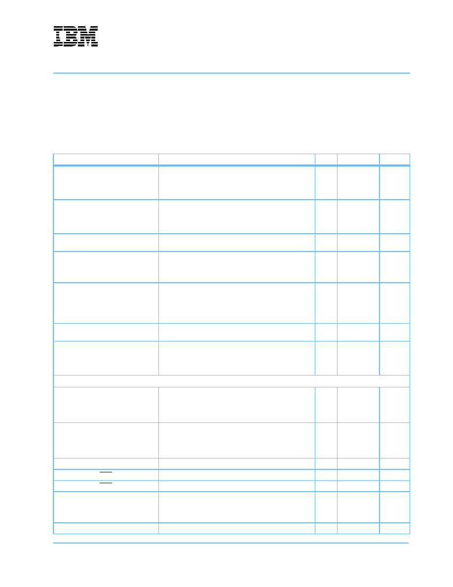
PHY0Col[PHY0Rx1Er]l
Collision [receive error] signal from the PHY. This is an
asynchronous signal (MII 0).
or
Receive Error ([RMII 1]).
I
5V tolerant
3.3V LVTTL
PHY0CrS[PHY0CrS0DV]
Carrier Sense signal from the PHY. This is an
asynchronous signal (MII 0).
or
Carrier sense data valid ([RMII 0]).
I
5V tolerant
3.3V LVTTL
1, 5
PHY0RxClk
Receiver medium clock. This signal is generated by the
PHY (MII 0).
I
5V tolerant
3.3V LVTTL
1, 4
PHY0RxD0[PHY0Rx0D0][PHY0Rx0D]
PHY0RxD1[PHY0Rx0D1][PHY0Rx1D]
PHY0RxD2[PHY0Rx1D0]
PHY0RxD3[PHY0Rx1D1]
Received Data. This is a nibble wide bus from the PHY.
The data is synchronous with PHY0RxClk
(MII 0[RMII 0, 1][SMII 0, 1]).
I
5V tolerant
3.3V LVTTL
1, 4
PHY0RxDV[PHY0CrS1DV]
Receive Data Valid. Data on the Data Bus is valid when
this signal is activated. Deassertion of this signal indicates
end of the frame reception (MII 0).
or
Carrier sense data valid ([RMII 1])
I
5V tolerant
3.3V LVTTL
1, 5
PHY0RxErr[PHY0Rx0Er]
Receive Error. This signal comes from the PHY and is
synchronous with PHY0RxClk (MII 0 [RMII 0]).
I
5V tolerant
3.3V LVTTL
1, 5
PHY0TxClk[PHY0RefClk]
Transmit medium clock. This signal is generated the PHY
([MII 0]).
or
Reference Clock [RMII and SMII].
I
5V tolerant
3.3V LVTTL
1, 4
SDRAM Interface
MemAddr00:31
Memory Data bus
Notes:
1. MemAddr00 is the most significant bit (msb).
2. MemData31 is the least significant bit (lsb).
I/O
3.3V LVTTL
MemAddr12:00
Memory Address bus.
Notes:
1. MemAddr12 is the most significant bit (msb).
2. MemAddr00 is the least significant bit (lsb).
O3.3V LVTTL
BA1:0
Bank Address supporting up to 4 internal banks
O
3.3V LVTTL
RAS
Row Address Strobe.
O
3.3V LVTTL
CAS
Column Address Strobe.
O
3.3V LVTTL
DQM0:3
DQM for byte lane 0 (MemAddr00:7),
1 (MemAddr08:15),
2 (MemData16:23), and
3 (MemData24:31)
O3.3V LVTTL
DQMCB
DQM for ECC check bits.
O
3.3V LVTTL
Signal Functional Description (Part 2 of 6)
Notes:
1. Receiver input has hysteresis.
2. Must pull up. See “Pull-up and Pull-down Resistors” on page 30 for recommended termination values.
3. Must pull down. See “Pull-up and Pull-down Resistors” on page 30 for recommended termination values.
4. If not used, must pull up.
5. If not used, must pull down.
6. Strapping input during reset; pull up or pull down as required.
7. Pull-up may be required. See “External Peripheral Bus Control Signals” on page 31.
Signal Name
Description
I/O
Type
Notes
相关PDF资料 |
PDF描述 |
|---|---|
| IBM25NPE405L-3FA266CZ | 32-BIT, 266 MHz, RISC PROCESSOR, PBGA324 |
| IBM25PPC405EP-3GB133CZ | 32-BIT, 133.33 MHz, RISC PROCESSOR, PBGA385 |
| IBM25PPC405EP-3GB133C | 32-BIT, 133.33 MHz, RISC PROCESSOR, PBGA385 |
| IBM25PPC405GP-3DD200C | RISC PROCESSOR, PBGA456 |
| IBM25PPC405GP-3BD266C | RISC PROCESSOR, PBGA456 |
相关代理商/技术参数 |
参数描述 |
|---|---|
| IBM25NPE405L-3FA266C | 制造商:AMCC 制造商全称:Applied Micro Circuits Corporation 功能描述:PowerNP |
| IBM25NPE405L-3FA266CZ | 制造商:AMCC 制造商全称:Applied Micro Circuits Corporation 功能描述:PowerNP |
| IBM25PPC403GAJC33C1 | 制造商:IBM 功能描述: |
| IBM25PPC405CR-3BC200C | 制造商:未知厂家 制造商全称:未知厂家 功能描述:MICROPROCESSOR|32-BIT|CMOS|BGA|316PIN|PLASTIC |
| IBM25PPC405CR-3BC200CZ | 制造商:未知厂家 制造商全称:未知厂家 功能描述:MICROPROCESSOR|32-BIT|CMOS|BGA|316PIN|PLASTIC |
发布紧急采购,3分钟左右您将得到回复。