- 您现在的位置:买卖IC网 > PDF目录20330 > ICL7673CBA (Intersil)IC SWITCH BATTERY BACKUP 8-SOIC PDF资料下载
参数资料
| 型号: | ICL7673CBA |
| 厂商: | Intersil |
| 文件页数: | 4/7页 |
| 文件大小: | 0K |
| 描述: | IC SWITCH BATTERY BACKUP 8-SOIC |
| 标准包装: | 1,960 |
| 应用: | 电池备份,工业/汽车,大电流开关 |
| FET 型: | N 和 P 沟道 |
| 输出数: | 1 |
| 内部开关: | 是 |
| 电源电压: | 2.5 V ~ 15 V |
| 电流 - 电源: | 1.5µA |
| 工作温度: | 0°C ~ 70°C |
| 安装类型: | 表面贴装 |
| 封装/外壳: | 8-SOIC(0.154",3.90mm 宽) |
| 供应商设备封装: | 8-SOICN |
| 包装: | 管件 |
�� �
�
�ICL7673�
�low� load� currents� the� output� voltage� is� nearly� equal� to� the�
�greater� of� the� two� inputs.� The� maximum� voltage� drop� across�
�switch� P� 1� or� P� 2� is� 0.5V,� since� above� this� voltage� the� body-�
�drain� parasitic� diode� will� become� forward� biased.� Complete�
�1mA�
�I� LOAD� =� 10mA�
�switching� of� the� inputs� and� open-drain� outputs� typically�
�occurs� in� 50� μ� s.�
�100mA�
�10nA�
�1nA�
�1000pA�
�V� S� =� 0V�
�85°C�
�Input� Voltage�
�The� input� operating� voltage� range� for� V� P� or� V� S� is� 2.5V� to�
�15V.� The� input� supply� voltage� (V� P� or� V� S� )� slew� rate� should� be�
�limited� to� 2V� per� microsecond� to� avoid� potential� harm� to� the�
�circuit.� In� line-operated� systems,� the� rate-of-rise� (or� fall)� of�
�the� supply� is� a� function� of� power� supply� design.� For� battery�
�applications� it� may� be� necessary� to� use� a� capacitor� between�
�the� input� and� ground� pins� to� limit� the� rate-of-rise� of� the�
�supply� voltage.� A� low-impedance� capacitor� such� as� a�
�0.047� μ� F� disc� ceramic� can� be� used� to� reduce� the� rate-of-rise.�
�Status� Indicator� Outputs�
�10pA�
�25°C�
�The� N-Channel� open� drain� output� transistors� can� be� used� to�
�indicate� which� supply� is� connected,� or� can� be� used� to� drive�
�external� PNP� transistors� to� increase� the� power� switching�
�capability� of� the� circuit.� When� using� external� PNP� power�
�1pA�
�0� 2� 4� 5� 6� 8� 10�
�INPUT� V� P� (V)�
�FIGURE� 5.� I� S� LEAKAGE� CURRENT� V� P� TO� V� S� AS� A�
�FUNCTION� OF� INPUT� VOLTAGE�
�12�
�transistors,� the� output� current� is� limited� by� the� beta� and�
�thermal� characteristics� of� the� power� transistors.� The�
�application� section� details� the� use� of� external� PNP�
�transistors.�
�Detailed� Description�
�As� shown� in� the� Functional� Diagram,� the� ICL7673� includes� a�
�comparator� which� senses� the� input� voltages� V� P� and� V� S� .� The�
�output� of� the� comparator� drives� the� first� inverter� and� the�
�open-drain� N-Channel� transistor� P� BAR� .� The� first� inverter�
�drives� a� large� P-Channel� switch,� P� 1� ,� a� second� inverter,� and�
�another� open-drain� N-Channel� transistor,� S� BAR� .� The� second�
�inverter� drives� another� large� P-Channel� switch� P� 2� .� The�
�ICL7673,� connected� to� a� main� and� a� backup� power� supply,�
�will� connect� the� supply� of� greater� potential� to� its� output.� The�
�circuit� provides� break-before-make� switch� action� as� it�
�switches� from� main� to� backup� power� in� the� event� of� a� main�
�power� supply� failure.� For� proper� operation,� inputs� V� P� and� V� S�
�must� not� be� allowed� to� float,� and,� the� difference� in� the� two�
�supplies� must� be� greater� than� 50mV.� The� leakage� current�
�through� the� reverse� biased� parasitic� diode� of� switch� P� 2� is�
�very� low.�
�Applications�
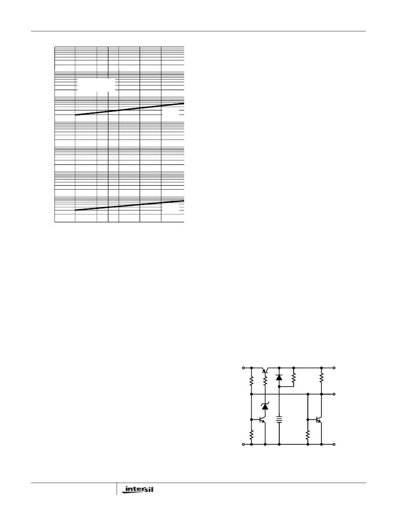
�A� typical� discrete� battery� backup� circuit� is� illustrated� in� Figure�
�6.� This� approach� requires� several� components,� substantial�
�printed� circuit� board� space,� and� high� labor� cost.� It� also�
�consumes� a� fairly� high� quiescent� current.� The� ICL7673�
�battery� backup� circuit,� illustrated� in� Figure� 7,� will� often� replace�
�such� discrete� designs� and� offer� much� better� performance,�
�higher� reliability,� and� lower� system� manufacturing� cost.� A�
�trickle� charge� system� could� be� implemented� with� an� additional�
�resistor� and� diode� as� shown� in� Figure� 8.� A� complete� low�
�power� AC� to� regulated� DC� system� can� be� implemented� using�
�the� ICL7673� and� ICL7663S� micropower� voltage� regulator� as�
�shown� in� Figure� 9.�
�+5V� V� O�
�PRIMARY� +5V� OR�
�DC� POWER� +3V�
�STATUS�
�INDICATOR�
�Output� Voltage�
�The� output� operating� voltage� range� is� 2.5V� to� 15V.� The�
�insertion� loss� between� either� input� and� the� output� is� a�
�function� of� load� current,� input� voltage,� and� temperature.� This�
�is� due� to� the� P-Channels� being� operated� in� their� triode�
�region,� and,� the� ON-resistance� of� the� switches� is� a� function�
�of� output� voltage� V� O� .� The� ON-resistance� of� the� P-Channels�
�have� positive� temperature� coefficients,� and� therefore� as�
�temperature� increases� the� insertion� loss� also� increases.� At�
�4�
�NiCAD�
�BATTERY�
�STACK�
�GND�
�FIGURE� 6.� DISCRETE� BATTERY� BACKUP� CIRCUIT�
�FN3183.4�
�July� 22,� 2005�
�相关PDF资料 |
PDF描述 |
|---|---|
| LM5051MAX/NOPB | IC ORING FET CTRLR 8SOIC |
| IR5001STRPBF | IC CTLR/MOSFET UNIV N-CH 8-SOIC |
| V24A3V3C200BF2 | CONVERTER MOD DC/DC 3.3V 200W |
| ECA15DTKN | CONN EDGECARD 30POS DIP .125 SLD |
| R2S-1524 | CONV DC/DC 2W 15VIN 24VOUT |
相关代理商/技术参数 |
参数描述 |
|---|---|
| ICL7673CBA-T | 功能描述:IC SWITCH BATTERY BACKUP 8-SOIC RoHS:否 类别:集成电路 (IC) >> PMIC - O 圈控制器 系列:- 标准包装:1,000 系列:- 应用:电池备份,工业/汽车,大电流开关 FET 型:- 输出数:5 内部开关:是 延迟时间 - 开启:100ns 延迟时间 - 关闭:- 电源电压:3 V ~ 5.5 V 电流 - 电源:250µA 工作温度:0°C ~ 70°C 安装类型:表面贴装 封装/外壳:16-SOIC(0.154",3.90mm 宽) 供应商设备封装:16-SOIC N 包装:带卷 (TR) |
| ICL7673CBAZA | 功能描述:电池管理 W/ANNEAL BATRY BCKUP SWITCH COM RoHS:否 制造商:Texas Instruments 电池类型:Li-Ion 输出电压:5 V 输出电流:4.5 A 工作电源电压:3.9 V to 17 V 最大工作温度:+ 85 C 最小工作温度:- 40 C 封装 / 箱体:VQFN-24 封装:Reel |
| ICL7673CBAZA-T | 功能描述:电池管理 W/ANNEAL BATRY BCKUP SWITCH COM TAPE & RoHS:否 制造商:Texas Instruments 电池类型:Li-Ion 输出电压:5 V 输出电流:4.5 A 工作电源电压:3.9 V to 17 V 最大工作温度:+ 85 C 最小工作温度:- 40 C 封装 / 箱体:VQFN-24 封装:Reel |
| ICL7673CPA | 功能描述:电池管理 BATRY BACKUP SWITCH COM RoHS:否 制造商:Texas Instruments 电池类型:Li-Ion 输出电压:5 V 输出电流:4.5 A 工作电源电压:3.9 V to 17 V 最大工作温度:+ 85 C 最小工作温度:- 40 C 封装 / 箱体:VQFN-24 封装:Reel |
| ICL7673CPA136 | 制造商:Harris Corporation 功能描述: |
发布紧急采购,3分钟左右您将得到回复。