- 您现在的位置:买卖IC网 > PDF目录65529 > ICS527R-02 (INTEGRATED DEVICE TECHNOLOGY INC) 527 SERIES, PLL BASED CLOCK DRIVER, 2 TRUE OUTPUT(S), 0 INVERTED OUTPUT(S), PDSO28 PDF资料下载
参数资料
| 型号: | ICS527R-02 |
| 厂商: | INTEGRATED DEVICE TECHNOLOGY INC |
| 元件分类: | 时钟及定时 |
| 英文描述: | 527 SERIES, PLL BASED CLOCK DRIVER, 2 TRUE OUTPUT(S), 0 INVERTED OUTPUT(S), PDSO28 |
| 封装: | 0.150 INCH, 0.635 MM PITCH, MO-153, SSOP-28 |
| 文件页数: | 4/9页 |
| 文件大小: | 255K |
| 代理商: | ICS527R-02 |
Clock Slicer User Configurable PECL Input Zero Delay Buffer
MDS 527-02 F
4
Revision 022806
Integrated Circuit Systems, Inc.
● 525 Race Street, San Jose, CA 95126 ● tel (408) 297-1201 ● www.icst.com
ICS527-02
the correct clock when mounted on the board. It is also
possible to connect the inputs to parallel I/O ports in
order to switch frequencies.
The output of the ICS527-02 can be determined by the
following simple equation:
Where:
Reference Divider Word (RDW) = 0 to 127
Feedback Divider Word (FDW) = 0 to 127
FB Frequency is the same as either CLK1 or
CLK2 depending on feedback connection
Also, the following operating ranges should be
observed:
S0 and S1 should be selected depending on the
frequency of CLK1. The table on page 2 gives the
ranges.
The dividers are expressed as integers. For example, if
a 50 MHz output on CLK1 is desired from a 40 MHz
input, the reference divider word (RDW) should be 2
and the feedback divider word (FDW) should be 3
which gives the required 5/4 multiplication. If multiple
choices of dividers are available, then the lowest
numbers should be used. In this example, the output
divide (OD) should be selected to be 2. Then R6:R0 is
0000010, F6:F0 is 0000011 and S1:S0 is 00. Also, this
example assumes CLK1 is connected to FBIN.
If you need assistance determining the optimum divider
settings, please send an e-mail to
mk-support@icst.com with the desired input clock and
the desired output frequency.
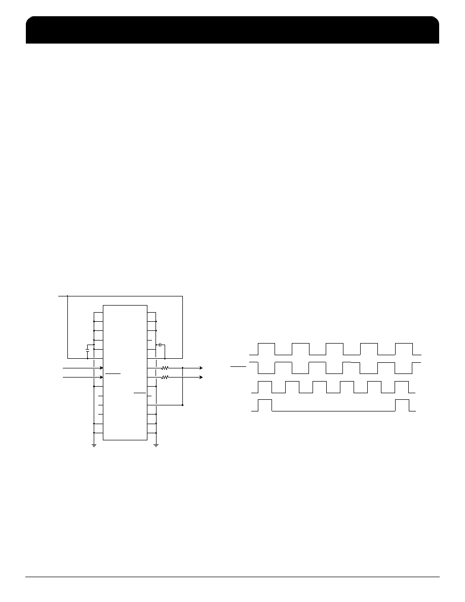
Typical Example
The layout diagram below will produce the waveforms shown on the right.
Note: The series termination resistor is located before the feedback trace
FB Frequency
Input Frequency
FDW
2
+
RDW
2
+
------------------------
×
=
300kHz
Input Frequency
RDW
2
+
-------------------------------------------
20 MHz
<<
40 MHz
PECLIN
50 MHz
CLK1
SYNC
CLK2
PECLIN
FBIN
PECLIN
F6
F5
GND
F4
OECLK2
F0
F1
F2
F3
CLK1
CLK2
GND
S1
VDD
R0
VDD
DIV2
S0
R2
R1
R5
R6
R4
R3
PECLIN
PDTS
50 MHz
SYNC
33
33
0.01
F
40 MHz
0.01
F
VDD
ICS527-02
Clock Slicer User Configurable PECL Input Zero Delay Buffer
TSD
IDT / ICS Clock Slicer User Configurable PECL Input Zero Delay Buffer
ICS527-02
4
相关PDF资料 |
PDF描述 |
|---|---|
| ICS527R-04LF | 527 SERIES, PLL BASED CLOCK DRIVER, 1 TRUE OUTPUT(S), 0 INVERTED OUTPUT(S), PDSO28 |
| ICS527R-04T | 527 SERIES, PLL BASED CLOCK DRIVER, 1 TRUE OUTPUT(S), 0 INVERTED OUTPUT(S), PDSO28 |
| ICS527R-04 | 527 SERIES, PLL BASED CLOCK DRIVER, 1 TRUE OUTPUT(S), 0 INVERTED OUTPUT(S), PDSO28 |
| ICS527R-04LFT | 527 SERIES, PLL BASED CLOCK DRIVER, 1 TRUE OUTPUT(S), 0 INVERTED OUTPUT(S), PDSO28 |
| ICS527R-04 | 527 SERIES, PLL BASED CLOCK DRIVER, 1 TRUE OUTPUT(S), 0 INVERTED OUTPUT(S), PDSO28 |
相关代理商/技术参数 |
参数描述 |
|---|---|
| ICS527R-02I | 功能描述:IC CLOCK SLICER ZD BUFFER 28SSOP RoHS:否 类别:集成电路 (IC) >> 时钟/计时 - 时钟发生器,PLL,频率合成器 系列:- 标准包装:1,000 系列:- 类型:时钟/频率合成器,扇出分配 PLL:- 输入:- 输出:- 电路数:- 比率 - 输入:输出:- 差分 - 输入:输出:- 频率 - 最大:- 除法器/乘法器:- 电源电压:- 工作温度:- 安装类型:表面贴装 封装/外壳:56-VFQFN 裸露焊盘 供应商设备封装:56-VFQFP-EP(8x8) 包装:带卷 (TR) 其它名称:844S012AKI-01LFT |
| ICS527R-02ILF | 制造商:Integrated Device Technology Inc 功能描述:IC CLOCK SLICER ZD BUFFER 28SSOP |
| ICS527R-02ILFT | 制造商:Integrated Device Technology Inc 功能描述:IC CLOCK SLICER ZD BUFFER 28SSOP |
| ICS527R-02IT | 功能描述:IC CLOCK SLICER ZD BUFFER 28SSOP RoHS:否 类别:集成电路 (IC) >> 时钟/计时 - 时钟发生器,PLL,频率合成器 系列:- 标准包装:1,000 系列:- 类型:时钟/频率合成器,扇出分配 PLL:- 输入:- 输出:- 电路数:- 比率 - 输入:输出:- 差分 - 输入:输出:- 频率 - 最大:- 除法器/乘法器:- 电源电压:- 工作温度:- 安装类型:表面贴装 封装/外壳:56-VFQFN 裸露焊盘 供应商设备封装:56-VFQFP-EP(8x8) 包装:带卷 (TR) 其它名称:844S012AKI-01LFT |
| ICS527R-02LF | 功能描述:IC CLK SLICER ZDB CONFIG 28-SSOP RoHS:是 类别:集成电路 (IC) >> 时钟/计时 - 时钟发生器,PLL,频率合成器 系列:- 标准包装:1,000 系列:- 类型:时钟/频率合成器,扇出分配 PLL:- 输入:- 输出:- 电路数:- 比率 - 输入:输出:- 差分 - 输入:输出:- 频率 - 最大:- 除法器/乘法器:- 电源电压:- 工作温度:- 安装类型:表面贴装 封装/外壳:56-VFQFN 裸露焊盘 供应商设备封装:56-VFQFP-EP(8x8) 包装:带卷 (TR) 其它名称:844S012AKI-01LFT |
发布紧急采购,3分钟左右您将得到回复。