- 您现在的位置:买卖IC网 > PDF目录65529 > ICS527R-04LFT 527 SERIES, PLL BASED CLOCK DRIVER, 1 TRUE OUTPUT(S), 0 INVERTED OUTPUT(S), PDSO28 PDF资料下载
参数资料
| 型号: | ICS527R-04LFT |
| 元件分类: | 时钟及定时 |
| 英文描述: | 527 SERIES, PLL BASED CLOCK DRIVER, 1 TRUE OUTPUT(S), 0 INVERTED OUTPUT(S), PDSO28 |
| 封装: | 0.150 INCH, 0.025 INCH PITCH, MO-153, SSOP-28 |
| 文件页数: | 5/9页 |
| 文件大小: | 165K |
| 代理商: | ICS527R-04LFT |
Clock Slicer User Configurable PECL input Zero Delay Buffer
MDS 527-04 D
5
Revision 122804
Integrated Circuit Systems, Inc.
● 525 Race Street, San Jose, CA 95126 ● tel (408) 297-1201 ● www.icst.com
ICS527-04
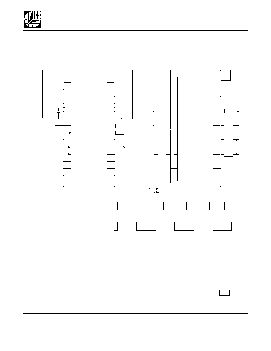
Multiple Output Example
In this example, an input clock of 125 MHz is used. Four low skew copies of 50 MHz PECL are required
aligned to the 125 MHz input clock. The following solution uses the ICS554-01A, which is a 1 to 4 PECL
buffer with low pin to pin skew.
Using the equation for selecting dividers gives:
If FDW = 0, then RDW = 3. This gives the required divide-by-5 function. Setting pin IRANGE = 1 (by leaving
it unconnected and using the internal pull-up) allows a higher speed input clock like the 125 MHz. The
FBPECL pair pins are connected to the Q1 outputs (chosen arbitrarily) of the ICS554. This aligns all the
outputs of the ICS554 with the 125 MHz input since the ICS527-04 aligns rising edges on the PECLIN and
FBPECL pins.
In this example, the resistor network needed for each PECLO output is represented by the
boxes.
125 MHz, PECLIN
50 MHz, PECLO
(Complementary outputs are not shown)
F6
FBPECL
F5
F4
GND
F3
PECLIN
F0
F1
F2
PECLO
GND
S1
VDD
R0
VDD
IRANGE
S0
R2
R1
R5
R6
R4
R3
FBPECL
RES
0.01 F
VDD
Q2
Q0
GND
Q1
GND
Q2
Q0
VDD
OE
NC
Q1
0.01 F
IC
S
55
4-
01A
IC
S
527-
04
The layout design above produces the waveforms shown below.
RN
50 MHz
125 MHz
RN
IN
Q3
RN
560
0.01 F
125 MHz
50 MHz = 125 MHz *
(FDW + 2)
(RDW + 2)
RN
相关PDF资料 |
PDF描述 |
|---|---|
| ICS527R-04 | 527 SERIES, PLL BASED CLOCK DRIVER, 1 TRUE OUTPUT(S), 0 INVERTED OUTPUT(S), PDSO28 |
| ICS541MT | PLL BASED CLOCK DRIVER, 2 TRUE OUTPUT(S), 0 INVERTED OUTPUT(S), PDSO8 |
| ICS544MI-01 | 156 MHz, OTHER CLOCK GENERATOR, PDSO8 |
| ICS544M-01LF | 156 MHz, OTHER CLOCK GENERATOR, PDSO8 |
| ICS544MI-01T | 156 MHz, OTHER CLOCK GENERATOR, PDSO8 |
相关代理商/技术参数 |
参数描述 |
|---|---|
| ICS527R-04T | 功能描述:IC CLK SLICER PECL ZDB 28-SSOP RoHS:否 类别:集成电路 (IC) >> 时钟/计时 - 时钟发生器,PLL,频率合成器 系列:- 产品变化通告:Product Discontinuation 04/May/2011 标准包装:96 系列:- 类型:时钟倍频器,零延迟缓冲器 PLL:带旁路 输入:LVTTL 输出:LVTTL 电路数:1 比率 - 输入:输出:1:8 差分 - 输入:输出:无/无 频率 - 最大:133.3MHz 除法器/乘法器:是/无 电源电压:3 V ~ 3.6 V 工作温度:0°C ~ 70°C 安装类型:表面贴装 封装/外壳:16-TSSOP(0.173",4.40mm 宽) 供应商设备封装:16-TSSOP 包装:管件 其它名称:23S08-5HPGG |
| ICS5300V-1 | 制造商:未知厂家 制造商全称:未知厂家 功能描述:Video DAC with Color Palette (RAMDAC) |
| ICS5300V-2 | 制造商:未知厂家 制造商全称:未知厂家 功能描述:Video DAC with Color Palette (RAMDAC) |
| ICS5300V-3 | 制造商:未知厂家 制造商全称:未知厂家 功能描述:Video DAC with Color Palette (RAMDAC) |
| ICS5301V-1 | 制造商:未知厂家 制造商全称:未知厂家 功能描述:Video DAC with Color Palette (RAMDAC) |
发布紧急采购,3分钟左右您将得到回复。