- 您现在的位置:买卖IC网 > PDF目录65529 > ICS544MI-01 156 MHz, OTHER CLOCK GENERATOR, PDSO8 PDF资料下载
参数资料
| 型号: | ICS544MI-01 |
| 元件分类: | 时钟产生/分配 |
| 英文描述: | 156 MHz, OTHER CLOCK GENERATOR, PDSO8 |
| 封装: | 0.150 INCH, SOIC-8 |
| 文件页数: | 2/7页 |
| 文件大小: | 142K |
| 代理商: | ICS544MI-01 |
Clock Divider
MDS 544M-01 A
2
Revision 041505
Integrated Circuit Systems, Inc.
● 525 Race Street, San Jose, CA 95126 ● tel (408) 297-1201 ● www.icst.com
ICS544-01
PRELIM INAR Y INFO RMA T ION
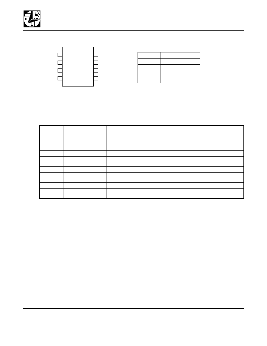
Pin Assignment
8-pin (150 mil) SOIC
Clock Divider Table
0 = connect directly to ground
1 = connect directly to VDD
Pin Descriptions
External Components
Series Termination Resistor
Clock output traces over one inch should use series
termination. To series terminate a 50
trace (a
commonly used trace impedance), place a 33
resistor
in series with the clock line, as close to the clock output
pin as possible. The nominal impedance of the clock
output is 20
.
On chip capacitors- Crystal capacitors should be
connected from pins X1 to ground and X2 to ground to
optimize the initial accuracy. The value (in pf) of these
crystal caps equal (CL-12)*2 in this equation,
CL=crystal load capacitance in pf. For example, for a
crystal with a 16 pF load cap, each external crystal cap
would be 8 pF. [(16-12)x2]=8.
Decoupling Capacitor
As with any high-performance mixed-signal IC, the
ICS544-01 must be isolated from system power supply
noise to perform optimally.
A decoupling capacitor of 0.01F must be connected
between VDD and the PCB ground plane.
PCB Layout Recommendations
For optimum device performance and lowest output
phase noise, the following guidelines should be
observed.
1) The 0.01F decoupling capacitor should be mounted
on the component side of the board as close to the
X1/ICLK
X2
GND
VDD
S0
OE
CLK
S1
1
2
3
4
8
7
6
5
S1
S0
CLK
0
Input/32
0
1
Input/64
10
Input/256
11
Input/512
Pin
Number
Pin
Name
Pin
Type
Pin Description
1
X1/ICLK
XI
Crystal or Clock input.
2
X2
Xo
Connect to crystal for crystal input and leave open for clock input.
3
GND
Power
Connect to ground.
4
S0
Input
Select 0 for output clock. Connect to GND or VDD, per divider table above.
Internal pull-up resistor.
5
CLK
Output
Clock output per table above.
6
OE
Input
Output Enable.Tri-states output clock when low. Also shuts down the oscillator
circuit. Internal pull-up resistor. OE=1 normal operation.
7
VDD
Power
Connect to 2.25 V to 3.6 V.
8
S1
Input
Select 1 for output clock. Connect to GND or VDD, per divider table above.
Internal pull-up resistor.
相关PDF资料 |
PDF描述 |
|---|---|
| ICS544M-01LF | 156 MHz, OTHER CLOCK GENERATOR, PDSO8 |
| ICS544MI-01T | 156 MHz, OTHER CLOCK GENERATOR, PDSO8 |
| ICS554-01DPK | 156 MHz, OTHER CLOCK GENERATOR, UUC |
| ICS548G-05LFT | 49.152 MHz, OTHER CLOCK GENERATOR, PDSO16 |
| ICS552G-02ILF | 552 SERIES, LOW SKEW CLOCK DRIVER, 8 TRUE OUTPUT(S), 0 INVERTED OUTPUT(S), PDSO16 |
相关代理商/技术参数 |
参数描述 |
|---|---|
| ICS544MI-01LF | 功能描述:IC CLK DIVIDER 16.777MHZ 8SOIC RoHS:是 类别:集成电路 (IC) >> 时钟/计时 - 时钟发生器,PLL,频率合成器 系列:ClockBlocks™ 标准包装:2,000 系列:- 类型:PLL 时钟发生器 PLL:带旁路 输入:LVCMOS,LVPECL 输出:LVCMOS 电路数:1 比率 - 输入:输出:2:11 差分 - 输入:输出:是/无 频率 - 最大:240MHz 除法器/乘法器:是/无 电源电压:3.135 V ~ 3.465 V 工作温度:0°C ~ 70°C 安装类型:表面贴装 封装/外壳:32-LQFP 供应商设备封装:32-TQFP(7x7) 包装:带卷 (TR) |
| ICS544MI-01LFT | 功能描述:IC CLK DIVIDER 16.777MHZ 8SOIC RoHS:是 类别:集成电路 (IC) >> 时钟/计时 - 时钟发生器,PLL,频率合成器 系列:ClockBlocks™ 标准包装:2,000 系列:- 类型:PLL 时钟发生器 PLL:带旁路 输入:LVCMOS,LVPECL 输出:LVCMOS 电路数:1 比率 - 输入:输出:2:11 差分 - 输入:输出:是/无 频率 - 最大:240MHz 除法器/乘法器:是/无 电源电压:3.135 V ~ 3.465 V 工作温度:0°C ~ 70°C 安装类型:表面贴装 封装/外壳:32-LQFP 供应商设备封装:32-TQFP(7x7) 包装:带卷 (TR) |
| ICS544MI-01T | 制造商:ICS 制造商全称:ICS 功能描述:Clock Divider |
| ICS548-03 | 制造商:ICS 制造商全称:ICS 功能描述:Low Skew Clock Inverter and Divider |
| ICS548-05A | 制造商:ICS 制造商全称:ICS 功能描述:PRELIMINARY INFORMATION MP3 Audio Clock |
发布紧急采购,3分钟左右您将得到回复。