- 您现在的位置:买卖IC网 > PDF目录65530 > ICS552G-03LFT (INTEGRATED DEVICE TECHNOLOGY INC) 552 SERIES, LOW SKEW CLOCK DRIVER, 8 TRUE OUTPUT(S), 0 INVERTED OUTPUT(S), PDSO16 PDF资料下载
参数资料
| 型号: | ICS552G-03LFT |
| 厂商: | INTEGRATED DEVICE TECHNOLOGY INC |
| 元件分类: | 时钟及定时 |
| 英文描述: | 552 SERIES, LOW SKEW CLOCK DRIVER, 8 TRUE OUTPUT(S), 0 INVERTED OUTPUT(S), PDSO16 |
| 封装: | 0.173 INCH, 0.65 MM PITCH, TSSOP-16 |
| 文件页数: | 2/6页 |
| 文件大小: | 99K |
| 代理商: | ICS552G-03LFT |
LOW SKEW 1 TO 8 CLOCK BUFFER (4 AT 1X, 4 AT 1/2X)
MDS 552-03 B
2
Revision 052501
Int egrat ed C i rcuit Syste ms q 525 R a ce S t r eet, San Jose, CA 95126 q t e l (40 8 ) 295 -9800 q
w w w. icst . c om
ICS552-03
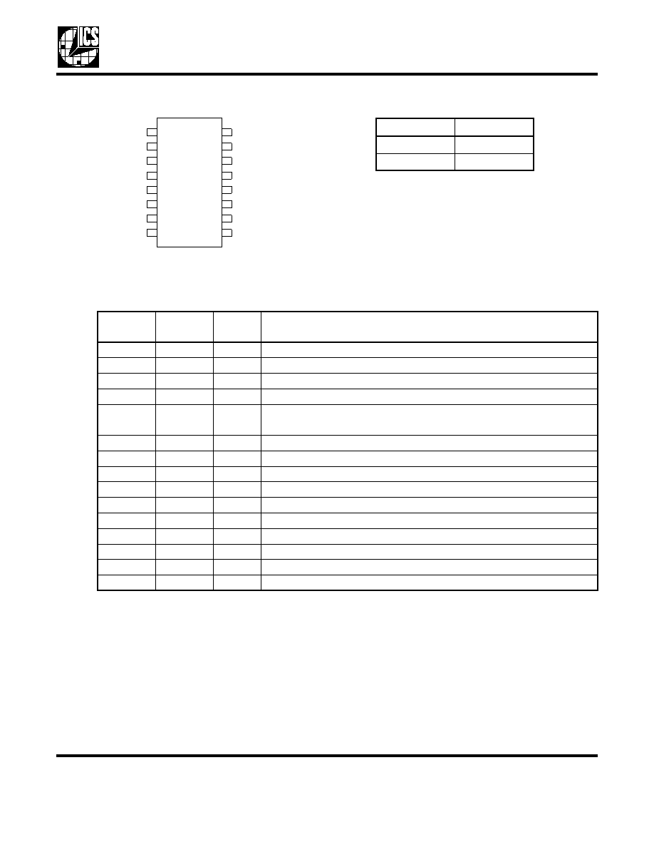
Pin Assignment
Input Source Select
Pin Descriptions
External Components
A minimum number of external components are required for proper operation. Decoupling capacitors of
0.01
F should be connected between VDD on pin 2 and GND on pin 7,and between VDD on pin 15 and
GND on pin 10, as close to the device as possible. A 33
series terminating resistor should be used on
each clock output if the trace is longer than 1 inch.
To achieve the low output skews that the ICS552-03 is capable of, careful attention must be paid to board
layout. Essentially, all 8 outputs must have identical terminations, identical loads, and identical trace
geometries. If they do not, the output skew will be degraded. For example, using a 30
series termination
on one output (with 33
on the others) will cause at least 15 ps of skew.
12
1
11
2
10
3
9
OE
4
VDD
5
Q0
6
VDD
7
Q1
8
Q2
P3
P2
P1
Q3
P0
INA
GND
16
15
14
13
INB
SELA
16 Pin 173 Mil (0.65mm) TSSOP
SELA
Input
0INB
1INA
Pin
Number
Pin
Name
Pin
Type
Pin Description
1
OE
Input
Output Enable. Tri-states outputs when low.Internal Pull-up resistor
2
VDD
Power
Connect to +2.5 V, +3.3 V or +5.0 V. Must be the same as pin 15
3
Q0
Output
Clock Output Q0
4
Q1
Output
Clock Output Q1
5
Q2
Output
Clock Output Q2
6
Q3
Output
Clock Output Q3
7
GND
Power
Ground
8
INB
Input
Clock Input B. 5 V tolerant input
9
INA
Input
Clock Input A. 5 V tolerant input
10
GND
Power
Ground
11
P0
Output
Clock Output P0
12
P1
Output
Clock Output P1
13
P2
Output
Clock Output P2
14
P3
Output
Clock Output P3
15
VDD
Power
Connect to +2.5 V, +3.3 V or +5.0 V. Must be the same as pin 2
16
SELA
Input
Selects either INA or INB. Internal pull-up resistor
相关PDF资料 |
PDF描述 |
|---|---|
| ICS552R-01T | LOW SKEW CLOCK DRIVER, PDSO20 |
| ICS552R-01 | LOW SKEW CLOCK DRIVER, PDSO20 |
| ICS552R-01T | LOW SKEW CLOCK DRIVER, PDSO20 |
| ICS552R-01I | LOW SKEW CLOCK DRIVER, PDSO20 |
| ICS552R-01IT | LOW SKEW CLOCK DRIVER, PDSO20 |
相关代理商/技术参数 |
参数描述 |
|---|---|
| ICS552G-03T | 制造商:ICS 制造商全称:ICS 功能描述:LOW SKEW 1 TO 8 CLOCK BUFFER (4 AT 1X, 4 AT 1/2X) |
| ICS552R-01 | 功能描述:IC OSC/MULT/BUFFER OCT 20-SSOP RoHS:否 类别:集成电路 (IC) >> 时钟/计时 - 时钟发生器,PLL,频率合成器 系列:- 产品变化通告:Product Discontinuation 04/May/2011 标准包装:96 系列:- 类型:时钟倍频器,零延迟缓冲器 PLL:带旁路 输入:LVTTL 输出:LVTTL 电路数:1 比率 - 输入:输出:1:8 差分 - 输入:输出:无/无 频率 - 最大:133.3MHz 除法器/乘法器:是/无 电源电压:3 V ~ 3.6 V 工作温度:0°C ~ 70°C 安装类型:表面贴装 封装/外壳:16-TSSOP(0.173",4.40mm 宽) 供应商设备封装:16-TSSOP 包装:管件 其它名称:23S08-5HPGG |
| ICS552R-01I | 功能描述:IC OSC/MULT/BUFFER OCT 20-SSOP RoHS:否 类别:集成电路 (IC) >> 时钟/计时 - 时钟发生器,PLL,频率合成器 系列:- 产品变化通告:Product Discontinuation 04/May/2011 标准包装:96 系列:- 类型:时钟倍频器,零延迟缓冲器 PLL:带旁路 输入:LVTTL 输出:LVTTL 电路数:1 比率 - 输入:输出:1:8 差分 - 输入:输出:无/无 频率 - 最大:133.3MHz 除法器/乘法器:是/无 电源电压:3 V ~ 3.6 V 工作温度:0°C ~ 70°C 安装类型:表面贴装 封装/外壳:16-TSSOP(0.173",4.40mm 宽) 供应商设备封装:16-TSSOP 包装:管件 其它名称:23S08-5HPGG |
| ICS552R-01ILF | 功能描述:IC OSC/MULT/BUFFER OCT 20-SSOP RoHS:是 类别:集成电路 (IC) >> 时钟/计时 - 时钟发生器,PLL,频率合成器 系列:- 标准包装:2,000 系列:- 类型:PLL 时钟发生器 PLL:带旁路 输入:LVCMOS,LVPECL 输出:LVCMOS 电路数:1 比率 - 输入:输出:2:11 差分 - 输入:输出:是/无 频率 - 最大:240MHz 除法器/乘法器:是/无 电源电压:3.135 V ~ 3.465 V 工作温度:0°C ~ 70°C 安装类型:表面贴装 封装/外壳:32-LQFP 供应商设备封装:32-TQFP(7x7) 包装:带卷 (TR) |
| ICS552R-01ILFT | 功能描述:IC OSC/MULT/BUFFER OCT 20-SSOP RoHS:是 类别:集成电路 (IC) >> 时钟/计时 - 时钟发生器,PLL,频率合成器 系列:- 标准包装:2,000 系列:- 类型:PLL 时钟发生器 PLL:带旁路 输入:LVCMOS,LVPECL 输出:LVCMOS 电路数:1 比率 - 输入:输出:2:11 差分 - 输入:输出:是/无 频率 - 最大:240MHz 除法器/乘法器:是/无 电源电压:3.135 V ~ 3.465 V 工作温度:0°C ~ 70°C 安装类型:表面贴装 封装/外壳:32-LQFP 供应商设备封装:32-TQFP(7x7) 包装:带卷 (TR) |
发布紧急采购,3分钟左右您将得到回复。