- 您现在的位置:买卖IC网 > PDF目录65530 > ICS554G-01AI (INTEGRATED DEVICE TECHNOLOGY INC) 554 SERIES, LOW SKEW CLOCK DRIVER, 4 TRUE OUTPUT(S), 0 INVERTED OUTPUT(S), PDSO16 PDF资料下载
参数资料
| 型号: | ICS554G-01AI |
| 厂商: | INTEGRATED DEVICE TECHNOLOGY INC |
| 元件分类: | 时钟及定时 |
| 英文描述: | 554 SERIES, LOW SKEW CLOCK DRIVER, 4 TRUE OUTPUT(S), 0 INVERTED OUTPUT(S), PDSO16 |
| 封装: | 4.40 MM, 0.65 MM PITCH, TSSOP-16 |
| 文件页数: | 3/7页 |
| 文件大小: | 175K |
| 代理商: | ICS554G-01AI |
ICS554-01A
LOW SKEW 1 TO 4 CLOCK BUFFER PECL IN, PECL OUT
PECL BUFFER
IDT / ICS LOW SKEW 1 TO 4 CLOCK BUFFER PECL IN, PECL OUT
3
ICS554-01A
REV B 070606
External Components
The ICS554-01A requires a decoupling capacitor of 0.01
F to be connected between VDD on pin 2 and GND on
pin 7, as well as between VDD on pin 15 and GND on pin 10. These decoupling capacitors should be placed as
close to the device as possible.
To achieve the low output skews that the ICS554-01A is capable of, careful attention must be paid to board layout.
Essentially, all 8 outputs must have identical terminations, loads, and trace geometries. If they do not, the output
skew will be degraded. For example, using a 30
series termination on one output (with 33 on the others) will
cause at least 15ps of skew.
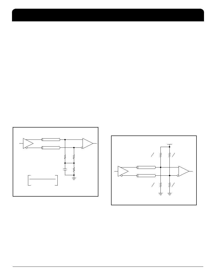
Termination for PECL or LVPECL Outputs
The clock layout topology shown below is a typical termination for PECL or LVPECL outputs. The two different
layouts mentioned are recommended only as guidelines.
FOUT and nFOUT are low impedance follower outputs that generate PECL/LVPECL compatible outputs.
Therefore, termination resistors (DC current path to ground) or current sources must be used for functionality.
These outputs are designed to drive 50 ohm transmission lines. Matched impedance techniques should be used to
maximize operating frequency and minimize signal distortion. There are a few simple termination schemes. The
figures below show two different layouts which are recommended only as guidelines. Other suitable clock layouts
may exist, but it is recommended that board designers simulate to guarantee compatibility across all printed circuit
and clock component process variations.
PECL or LVPECL Output Termination
LVPECL Output Termination
Z
0 = 50 ohms
F
OUT
F
IN
Z
0 = 50 ohms
50 ohms
C1
RTT
RTT =
Z
0
(V
OH + VOL / VCC -2) -2
1
C1 = 0.1F to 0.01F
Z
0 = 50 ohms
F
OUT
F
IN
Z
0 = 50 ohms
Z
0
3.3 V
5
2
3 2
5
2
Z
0
Z
0
3 2 Z
0
相关PDF资料 |
PDF描述 |
|---|---|
| ICS554G-01IT | LOW SKEW CLOCK DRIVER, 4 TRUE OUTPUT(S), 0 INVERTED OUTPUT(S), PDSO16 |
| ICS557G-06LFT | 557 SERIES, LOW SKEW CLOCK DRIVER, 4 TRUE OUTPUT(S), 0 INVERTED OUTPUT(S), PDSO20 |
| ICS557G-06T | 557 SERIES, LOW SKEW CLOCK DRIVER, 4 TRUE OUTPUT(S), 0 INVERTED OUTPUT(S), PDSO20 |
| ICS557G-07T | 557 SERIES, LOW SKEW CLOCK DRIVER, 1 TRUE OUTPUT(S), 0 INVERTED OUTPUT(S), PDSO16 |
| ICS557G-07 | 557 SERIES, LOW SKEW CLOCK DRIVER, 1 TRUE OUTPUT(S), 0 INVERTED OUTPUT(S), PDSO16 |
相关代理商/技术参数 |
参数描述 |
|---|---|
| ICS554G-01AILF | 功能描述:IC CLK BUFFER 1:4 200MHZ 16TSSOP RoHS:是 类别:集成电路 (IC) >> 时钟/计时 - 时钟缓冲器,驱动器 系列:ClockBlocks™ 标准包装:1 系列:HiPerClockS™ 类型:扇出缓冲器(分配),多路复用器 电路数:1 比率 - 输入:输出:2:18 差分 - 输入:输出:是/无 输入:CML,LVCMOS,LVPECL,LVTTL,SSTL 输出:LVCMOS,LVTTL 频率 - 最大:250MHz 电源电压:2.375 V ~ 3.465 V 工作温度:0°C ~ 70°C 安装类型:表面贴装 封装/外壳:32-LQFP 供应商设备封装:32-TQFP(7x7) 包装:- 其它名称:800-1923-6 |
| ICS554G-01AILFT | 功能描述:IC CLK BUFFER 1:4 200MHZ 16TSSOP RoHS:是 类别:集成电路 (IC) >> 时钟/计时 - 时钟缓冲器,驱动器 系列:ClockBlocks™ 标准包装:1 系列:HiPerClockS™ 类型:扇出缓冲器(分配),多路复用器 电路数:1 比率 - 输入:输出:2:18 差分 - 输入:输出:是/无 输入:CML,LVCMOS,LVPECL,LVTTL,SSTL 输出:LVCMOS,LVTTL 频率 - 最大:250MHz 电源电压:2.375 V ~ 3.465 V 工作温度:0°C ~ 70°C 安装类型:表面贴装 封装/外壳:32-LQFP 供应商设备封装:32-TQFP(7x7) 包装:- 其它名称:800-1923-6 |
| ICS554G-01AIT | 功能描述:IC CLK BUFFER 1:4 200MHZ 16TSSOP RoHS:否 类别:集成电路 (IC) >> 时钟/计时 - 时钟缓冲器,驱动器 系列:ClockBlocks™ 标准包装:1 系列:HiPerClockS™ 类型:扇出缓冲器(分配),多路复用器 电路数:1 比率 - 输入:输出:2:18 差分 - 输入:输出:是/无 输入:CML,LVCMOS,LVPECL,LVTTL,SSTL 输出:LVCMOS,LVTTL 频率 - 最大:250MHz 电源电压:2.375 V ~ 3.465 V 工作温度:0°C ~ 70°C 安装类型:表面贴装 封装/外壳:32-LQFP 供应商设备封装:32-TQFP(7x7) 包装:- 其它名称:800-1923-6 |
| ICS554G-01T | 制造商:ICS 制造商全称:ICS 功能描述:LOW SKEW 1 TO 4 CLOCK BUFFER PECL IN, PECL OUT |
| ICS554GI-01A | 制造商:ICS 制造商全称:ICS 功能描述:LOW SKEW 1 TO 4 CLOCK BUFFER PECL IN, PECL OUT |
发布紧急采购,3分钟左右您将得到回复。