- 您现在的位置:买卖IC网 > PDF目录65530 > ICS570ALF 570 SERIES, PLL BASED CLOCK DRIVER, 2 TRUE OUTPUT(S), 0 INVERTED OUTPUT(S), PDSO8 PDF资料下载
参数资料
| 型号: | ICS570ALF |
| 元件分类: | 时钟及定时 |
| 英文描述: | 570 SERIES, PLL BASED CLOCK DRIVER, 2 TRUE OUTPUT(S), 0 INVERTED OUTPUT(S), PDSO8 |
| 封装: | 0.150 INCH, LEAD FREE, SOIC-8 |
| 文件页数: | 1/9页 |
| 文件大小: | 199K |
| 代理商: | ICS570ALF |
ICS570
MDS 570 I
1
Revision 030905
Integrated Circuit Systems, Inc.
● 525 Race Street, San Jose, CA 95126 ● tel (408) 297-1201 ● www.icst.com
Multiplier and Zero Delay Buffer
Description
The ICS570 is a high-performance Zero Delay Buffer
(ZDB) which integrates ICS’ proprietary analog/digital
Phase Locked Loop (PLL) techniques. The A version is
recommended for 5 V designs and the B version for
3.3 V designs. The chip is part of ICS’ ClockBlocksTM
family, and was designed as a performance upgrade to
meet today’s higher speed and lower voltage
requirements. The zero delay feature means that the
rising edge of the input clock aligns with the rising
edges of both output clocks, giving the appearance of
no delay through the device. There are two outputs on
the chip, one being a low-skew divide by two of the
other output. The device incorporates an all-chip power
down/tri-state mode that stops the internal PLL and
puts both outputs into a high impedance state.
The ICS570 is ideal for synchronizing outputs in a large
variety of systems, from personal computers to data
communications to graphics/video. By allowing off-chip
feedback paths, the device can eliminate the delay
through other devices.
The ICS570 A and B versions were designed to
improve input to output jitter from the original ICS570M
version, and are recommended for all new designs.
Features
8-pin SOIC package
Available in Pb (lead) free package (A and B versions
only)
Pin-for-pin replacement and upgrade to ICS570M
Functional equivalent to AV9170 (not a pin-for-pin
replacement)
Low input to output skew of 300 ps max (>60 MHz
outputs)
Ability to choose between 14 different multipliers
from 0.5x to 32x
Output clock frequency up to 168 MHz at 3.3 V
Can recover degraded input clock duty cycle
Output clock duty cycle of 45/55
Power Down and Tri-State Mode
Passes spread spectrum clock modulation
Full CMOS clock swings with 25 mA drive capability
at TTL levels
Advanced, low power CMOS process
ICS570B has an operating voltage of 3.3 V (±5%)
ICS570A has an operating voltage of 5.0 V (±5%)
Industrial temperature version available
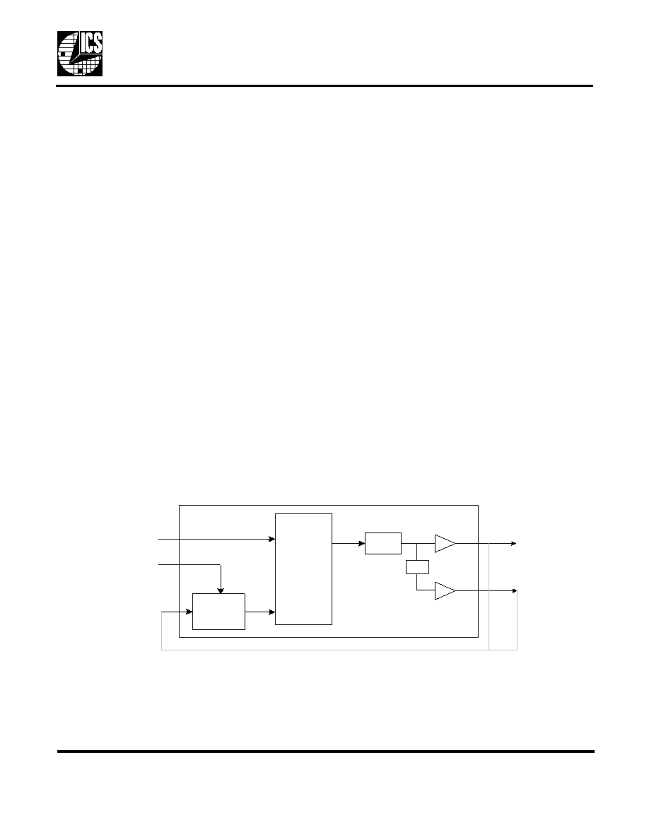
Block Diagram
Ph as e
Detec tor,
C harge
Pum p,
and Loop
F ilter
divide
by N
CL K
E xte rn al fe ed ba ck ca n c o m e from C L K or C L K /2 (s ee ta b le on pa ge 2 )
IC L K
FBIN
S1 :0
VC O
CL K 2
/2
相关PDF资料 |
PDF描述 |
|---|---|
| ICS570B | 570 SERIES, PLL BASED CLOCK DRIVER, 2 TRUE OUTPUT(S), 0 INVERTED OUTPUT(S), PDSO8 |
| ICS570GI-01LF | 570 SERIES, PLL BASED CLOCK DRIVER, 1 TRUE OUTPUT(S), 0 INVERTED OUTPUT(S), PDSO8 |
| ICS570GI-01LFT | 570 SERIES, PLL BASED CLOCK DRIVER, 1 TRUE OUTPUT(S), 0 INVERTED OUTPUT(S), PDSO8 |
| ICS571MLFT | 571 SERIES, PLL BASED CLOCK DRIVER, 2 TRUE OUTPUT(S), 0 INVERTED OUTPUT(S), PDSO8 |
| ICS571MT | 571 SERIES, PLL BASED CLOCK DRIVER, 2 TRUE OUTPUT(S), 0 INVERTED OUTPUT(S), PDSO8 |
相关代理商/技术参数 |
参数描述 |
|---|---|
| ICS570ALFT | 功能描述:IC MULTIPLIER/ZDB 8-SOIC RoHS:是 类别:集成电路 (IC) >> 时钟/计时 - 时钟发生器,PLL,频率合成器 系列:ClockBlocks™ 标准包装:2,000 系列:- 类型:PLL 时钟发生器 PLL:带旁路 输入:LVCMOS,LVPECL 输出:LVCMOS 电路数:1 比率 - 输入:输出:2:11 差分 - 输入:输出:是/无 频率 - 最大:240MHz 除法器/乘法器:是/无 电源电压:3.135 V ~ 3.465 V 工作温度:0°C ~ 70°C 安装类型:表面贴装 封装/外壳:32-LQFP 供应商设备封装:32-TQFP(7x7) 包装:带卷 (TR) |
| ICS570AT | 功能描述:IC MULTIPLIER/ZDB 8-SOIC RoHS:否 类别:集成电路 (IC) >> 时钟/计时 - 时钟发生器,PLL,频率合成器 系列:ClockBlocks™ 产品变化通告:Product Discontinuation 04/May/2011 标准包装:96 系列:- 类型:时钟倍频器,零延迟缓冲器 PLL:带旁路 输入:LVTTL 输出:LVTTL 电路数:1 比率 - 输入:输出:1:8 差分 - 输入:输出:无/无 频率 - 最大:133.3MHz 除法器/乘法器:是/无 电源电压:3 V ~ 3.6 V 工作温度:0°C ~ 70°C 安装类型:表面贴装 封装/外壳:16-TSSOP(0.173",4.40mm 宽) 供应商设备封装:16-TSSOP 包装:管件 其它名称:23S08-5HPGG |
| ICS570B | 功能描述:IC MULTIPLIER/ZDB 8-SOIC RoHS:否 类别:集成电路 (IC) >> 时钟/计时 - 时钟发生器,PLL,频率合成器 系列:ClockBlocks™ 产品变化通告:Product Discontinuation 04/May/2011 标准包装:96 系列:- 类型:时钟倍频器,零延迟缓冲器 PLL:带旁路 输入:LVTTL 输出:LVTTL 电路数:1 比率 - 输入:输出:1:8 差分 - 输入:输出:无/无 频率 - 最大:133.3MHz 除法器/乘法器:是/无 电源电压:3 V ~ 3.6 V 工作温度:0°C ~ 70°C 安装类型:表面贴装 封装/外壳:16-TSSOP(0.173",4.40mm 宽) 供应商设备封装:16-TSSOP 包装:管件 其它名称:23S08-5HPGG |
| ICS570BI | 功能描述:IC MULTIPLIER/ZDB 8-SOIC RoHS:否 类别:集成电路 (IC) >> 时钟/计时 - 时钟发生器,PLL,频率合成器 系列:ClockBlocks™ 产品变化通告:Product Discontinuation 04/May/2011 标准包装:96 系列:- 类型:时钟倍频器,零延迟缓冲器 PLL:带旁路 输入:LVTTL 输出:LVTTL 电路数:1 比率 - 输入:输出:1:8 差分 - 输入:输出:无/无 频率 - 最大:133.3MHz 除法器/乘法器:是/无 电源电压:3 V ~ 3.6 V 工作温度:0°C ~ 70°C 安装类型:表面贴装 封装/外壳:16-TSSOP(0.173",4.40mm 宽) 供应商设备封装:16-TSSOP 包装:管件 其它名称:23S08-5HPGG |
| ICS570BILF | 功能描述:IC MULTIPLIER/ZDB 8-SOIC RoHS:是 类别:集成电路 (IC) >> 时钟/计时 - 时钟发生器,PLL,频率合成器 系列:ClockBlocks™ 标准包装:2,000 系列:- 类型:PLL 频率合成器 PLL:是 输入:晶体 输出:时钟 电路数:1 比率 - 输入:输出:1:1 差分 - 输入:输出:无/无 频率 - 最大:1GHz 除法器/乘法器:是/无 电源电压:4.5 V ~ 5.5 V 工作温度:-20°C ~ 85°C 安装类型:表面贴装 封装/外壳:16-LSSOP(0.175",4.40mm 宽) 供应商设备封装:16-SSOP 包装:带卷 (TR) 其它名称:NJW1504V-TE1-NDNJW1504V-TE1TR |
发布紧急采购,3分钟左右您将得到回复。