- 您现在的位置:买卖IC网 > PDF目录65530 > ICS571MLF (INTEGRATED DEVICE TECHNOLOGY INC) 571 SERIES, PLL BASED CLOCK DRIVER, 2 TRUE OUTPUT(S), 0 INVERTED OUTPUT(S), PDSO8 PDF资料下载
参数资料
| 型号: | ICS571MLF |
| 厂商: | INTEGRATED DEVICE TECHNOLOGY INC |
| 元件分类: | 时钟及定时 |
| 英文描述: | 571 SERIES, PLL BASED CLOCK DRIVER, 2 TRUE OUTPUT(S), 0 INVERTED OUTPUT(S), PDSO8 |
| 封装: | 0.150 INCH, ROHS COMPLIANT, SOIC-8 |
| 文件页数: | 1/7页 |
| 文件大小: | 184K |
| 代理商: | ICS571MLF |
DATASHEET
LOW PHASE NOISE ZERO DELAY BUFFER
ICS571
IDT / ICS LOW PHASE NOISE ZERO DELAY BUFFER
1
ICS571
REV F 062306
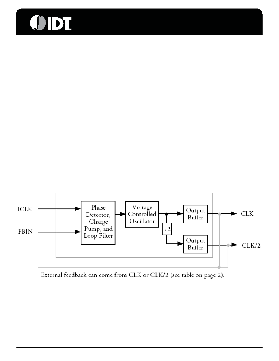
Description
The ICS571 is a high speed, high output drive, low phase
noise Zero Delay Buffer (ZDB) which integrates ICS’
proprietary analog/digital Phase Locked Loop (PLL)
techniques. ICS introduced the world standard for these
devices in 1992 with the debut of the AV9170, and updated
that with the ICS570. The ICS571, part of ICS’
ClockBlocks family, was designed to operate at higher
frequencies, with faster rise and fall times, and with lower
phase noise. The zero delay feature means that the rising
edge of the input clock aligns with the rising edges of both
outputs, giving the appearance of no delay through the
device. There are two outputs on the chip, one being a
low-skew divide by two of the other.
The chip is ideal for synchronizing outputs in a large variety
of systems, from personal computers to data
communications to video. By allowing offchip feedback
paths, the ICS571 can eliminate the delay through other
devices. The use of dividers in the feedback path will enable
the part to multiply by more than two.
Features
Packaged in 8-pin SOIC (Pb free available)
Can function as low phase noise x2 multiplier
Low skew outputs. One is ÷2 of other
Input clock frequency up to 160 MHz at 3.3 V
Phase noise of better than -100 dBc/Hz from 1 kHz to 1
MHz offset from carrier
Can recover poor input clock duty cycle
Output clock duty cycle of 45/55 at 3.3 V
High drive strength for >100 MHz outputs
Full CMOS clock swings with 25 mA drive capability at
TTL levels
Advanced, low power CMOS process
Operating voltages of 3.0 to 5.5 V
Block Diagram
相关PDF资料 |
PDF描述 |
|---|---|
| ICS571M | 571 SERIES, PLL BASED CLOCK DRIVER, 2 TRUE OUTPUT(S), 0 INVERTED OUTPUT(S), PDSO8 |
| ICS574MILF | 574 SERIES, PLL BASED CLOCK DRIVER, 4 TRUE OUTPUT(S), 0 INVERTED OUTPUT(S), PDSO8 |
| ICS574MLFT | 574 SERIES, PLL BASED CLOCK DRIVER, 4 TRUE OUTPUT(S), 0 INVERTED OUTPUT(S), PDSO8 |
| ICS574M | 574 SERIES, PLL BASED CLOCK DRIVER, 4 TRUE OUTPUT(S), 0 INVERTED OUTPUT(S), PDSO8 |
| ICS574MLFT | 574 SERIES, PLL BASED CLOCK DRIVER, 4 TRUE OUTPUT(S), 0 INVERTED OUTPUT(S), PDSO8 |
相关代理商/技术参数 |
参数描述 |
|---|---|
| ICS571MLFT | 功能描述:IC BUFFER ZD LOW PH/NOISE 8-SOIC RoHS:是 类别:集成电路 (IC) >> 时钟/计时 - 时钟发生器,PLL,频率合成器 系列:ClockBlocks™ 标准包装:2,000 系列:- 类型:PLL 时钟发生器 PLL:带旁路 输入:LVCMOS,LVPECL 输出:LVCMOS 电路数:1 比率 - 输入:输出:2:11 差分 - 输入:输出:是/无 频率 - 最大:240MHz 除法器/乘法器:是/无 电源电压:3.135 V ~ 3.465 V 工作温度:0°C ~ 70°C 安装类型:表面贴装 封装/外壳:32-LQFP 供应商设备封装:32-TQFP(7x7) 包装:带卷 (TR) |
| ICS571MT | 功能描述:IC MULTIPLIER/ZDB 8-SOIC RoHS:否 类别:集成电路 (IC) >> 时钟/计时 - 时钟发生器,PLL,频率合成器 系列:ClockBlocks™ 产品变化通告:Product Discontinuation 04/May/2011 标准包装:96 系列:- 类型:时钟倍频器,零延迟缓冲器 PLL:带旁路 输入:LVTTL 输出:LVTTL 电路数:1 比率 - 输入:输出:1:8 差分 - 输入:输出:无/无 频率 - 最大:133.3MHz 除法器/乘法器:是/无 电源电压:3 V ~ 3.6 V 工作温度:0°C ~ 70°C 安装类型:表面贴装 封装/外壳:16-TSSOP(0.173",4.40mm 宽) 供应商设备封装:16-TSSOP 包装:管件 其它名称:23S08-5HPGG |
| ICS574 | 制造商:ICS 制造商全称:ICS 功能描述:Zero Delay, Low Skew Buffer |
| ICS574M | 功能描述:IC CLOCK ZDB 1:4 160MHZ 8SOIC RoHS:否 类别:集成电路 (IC) >> 时钟/计时 - 时钟发生器,PLL,频率合成器 系列:- 产品变化通告:Product Discontinuation 04/May/2011 标准包装:96 系列:- 类型:时钟倍频器,零延迟缓冲器 PLL:带旁路 输入:LVTTL 输出:LVTTL 电路数:1 比率 - 输入:输出:1:8 差分 - 输入:输出:无/无 频率 - 最大:133.3MHz 除法器/乘法器:是/无 电源电压:3 V ~ 3.6 V 工作温度:0°C ~ 70°C 安装类型:表面贴装 封装/外壳:16-TSSOP(0.173",4.40mm 宽) 供应商设备封装:16-TSSOP 包装:管件 其它名称:23S08-5HPGG |
| ICS574MI | 功能描述:IC CLOCK ZDB 1:4 160MHZ 8SOIC RoHS:否 类别:集成电路 (IC) >> 时钟/计时 - 时钟发生器,PLL,频率合成器 系列:- 产品变化通告:Product Discontinuation 04/May/2011 标准包装:96 系列:- 类型:时钟倍频器,零延迟缓冲器 PLL:带旁路 输入:LVTTL 输出:LVTTL 电路数:1 比率 - 输入:输出:1:8 差分 - 输入:输出:无/无 频率 - 最大:133.3MHz 除法器/乘法器:是/无 电源电压:3 V ~ 3.6 V 工作温度:0°C ~ 70°C 安装类型:表面贴装 封装/外壳:16-TSSOP(0.173",4.40mm 宽) 供应商设备封装:16-TSSOP 包装:管件 其它名称:23S08-5HPGG |
发布紧急采购,3分钟左右您将得到回复。