- 您现在的位置:买卖IC网 > PDF目录65530 > ICS580M-01 580 SERIES, LOW SKEW CLOCK DRIVER, 2 TRUE OUTPUT(S), 0 INVERTED OUTPUT(S), PDSO16 PDF资料下载
参数资料
| 型号: | ICS580M-01 |
| 元件分类: | 时钟及定时 |
| 英文描述: | 580 SERIES, LOW SKEW CLOCK DRIVER, 2 TRUE OUTPUT(S), 0 INVERTED OUTPUT(S), PDSO16 |
| 封装: | 0.150 INCH, SOIC-16 |
| 文件页数: | 4/8页 |
| 文件大小: | 152K |
| 代理商: | ICS580M-01 |
Glitch-Free Clock Multiplexer
MDS 580-01 E
4
Revision 080305
Integrated Circuit Systems, Inc.
● 525 Race Street, San Jose, CA 95126 ● tel (408) 297-1201 ● www.icst.com
ICS580-01
Application Example
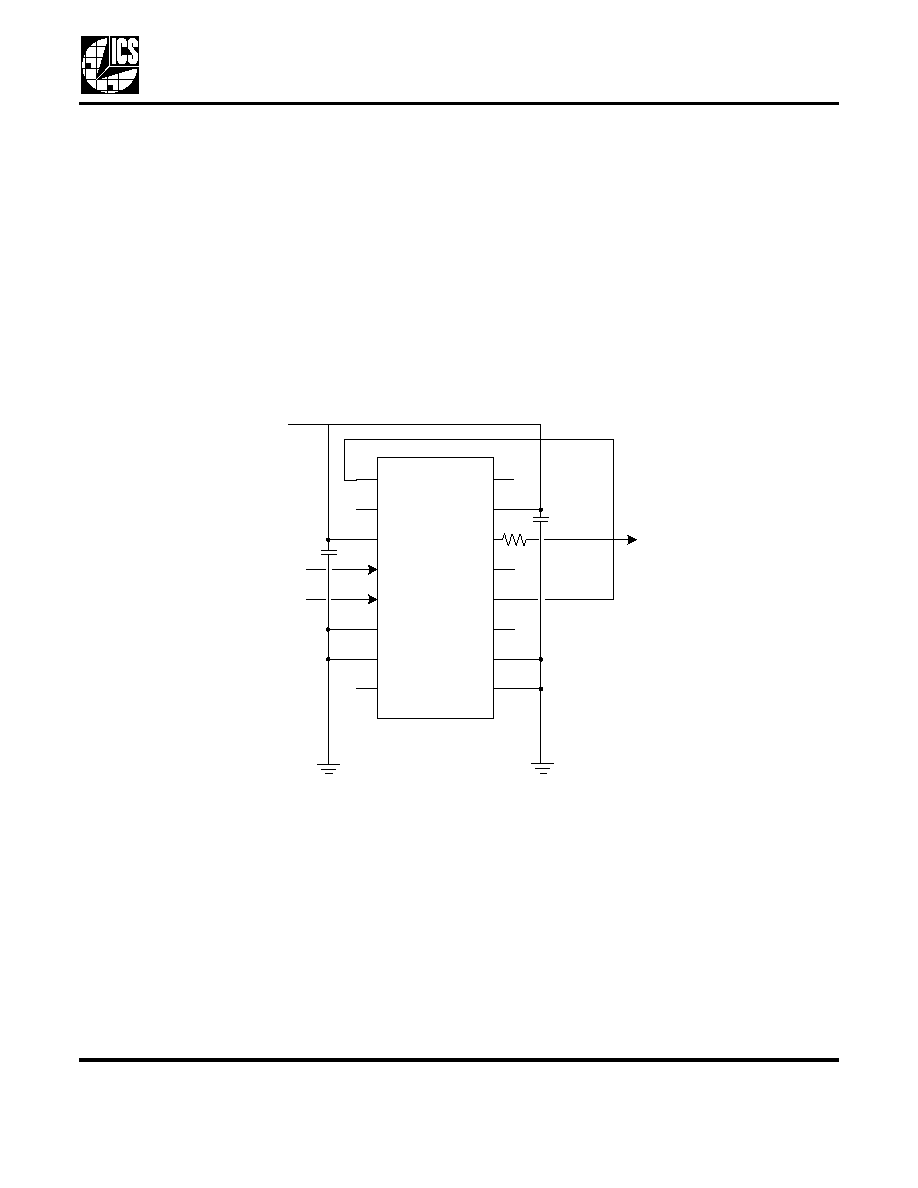
In the third example, the ICS580-01 is configured to automatically switch clocks when an input stops. The
clock that could stop is connected to INA while the backup clock (always running) is connected to INB. The
output NO_INA is connected to SELB. This means that when the clock on INA stops, NO_INA goes high
selecting the clock on INB which is muxed to the output after three cycles. When the clock on INA restarts,
NO_INA immediately goes low, selecting the clock on INA. The output then switches in the manner
described in the first example.
The circuit diagram in Figure 3 shows a typical connection for this example. Note that CLK2 and NO_INB
are unused and are disabled by grounding OE2 and OE4. A 33
series termination resistor is used on the
clock output and two decoupling capacitors of 0.01
F are used. All other inputs are left floating and are
therefore pulled high by the on-chip pull-ups.
Output Enable
Each output has a dedicated output enable pin. If an output is unused, it should be tri-stated by tying the
appropriate output enable pin to ground.
External Components
The ICS580-01 requires two 0.01
F decoupling capacitors, one between VDDI and GND and one between
VDDC and GND. Series termination resistors of 33
can be used on CLK1 and CLK2.
NO_INA
SELB
NO_INB
DIV
GND
VDDI
OE2
INA
INB
GND
OE4
OE3
OE1
VDDC
CLK1
CLK2
VDD
0.01
F
33
0.01
F
Normal Clock
Backup Clock
Output Clock
相关PDF资料 |
PDF描述 |
|---|---|
| ICS5OSK481TILF | 5OSK SERIES, PLL BASED CLOCK DRIVER, 1 TRUE OUTPUT(S), 0 INVERTED OUTPUT(S), PDSO5 |
| ICS601G-21LFT | 220 MHz, OTHER CLOCK GENERATOR, PDSO16 |
| ICS601G-21T | 220 MHz, OTHER CLOCK GENERATOR, PDSO16 |
| ICS601M-01T | 156 MHz, OTHER CLOCK GENERATOR, PDSO16 |
| ICS601G-01IT | 156 MHz, OTHER CLOCK GENERATOR, PDSO16 |
相关代理商/技术参数 |
参数描述 |
|---|---|
| ICS580M-01I | 功能描述:IC CLK MUX ZERO DLAY BUFF 16SOIC RoHS:否 类别:集成电路 (IC) >> 时钟/计时 - 时钟缓冲器,驱动器 系列:- 标准包装:1 系列:HiPerClockS™ 类型:扇出缓冲器(分配),多路复用器 电路数:1 比率 - 输入:输出:2:18 差分 - 输入:输出:是/无 输入:CML,LVCMOS,LVPECL,LVTTL,SSTL 输出:LVCMOS,LVTTL 频率 - 最大:250MHz 电源电压:2.375 V ~ 3.465 V 工作温度:0°C ~ 70°C 安装类型:表面贴装 封装/外壳:32-LQFP 供应商设备封装:32-TQFP(7x7) 包装:- 其它名称:800-1923-6 |
| ICS580M-01ILF | 功能描述:IC CLK MUX ZERO DLAY BUFF 16SOIC RoHS:是 类别:集成电路 (IC) >> 时钟/计时 - 时钟缓冲器,驱动器 系列:- 产品培训模块:High Bandwidth Product Overview 标准包装:1,000 系列:Precision Edge® 类型:扇出缓冲器(分配) 电路数:1 比率 - 输入:输出:1:4 差分 - 输入:输出:是/是 输入:CML,LVDS,LVPECL 输出:CML 频率 - 最大:2.5GHz 电源电压:2.375 V ~ 2.625 V 工作温度:-40°C ~ 85°C 安装类型:表面贴装 封装/外壳:16-VFQFN 裸露焊盘,16-MLF? 供应商设备封装:16-MLF?(3x3) 包装:带卷 (TR) |
| ICS580M-01ILFT | 功能描述:IC CLK MUX ZERO DLAY BUFF 16SOIC RoHS:是 类别:集成电路 (IC) >> 时钟/计时 - 时钟缓冲器,驱动器 系列:- 标准包装:74 系列:- 类型:扇出缓冲器(分配) 电路数:1 比率 - 输入:输出:1:10 差分 - 输入:输出:是/是 输入:HCSL, LVCMOS, LVDS, LVPECL, LVTTL 输出:HCSL,LVDS 频率 - 最大:400MHz 电源电压:3 V ~ 3.6 V 工作温度:-40°C ~ 85°C 安装类型:表面贴装 封装/外壳:32-VFQFN 裸露焊盘 供应商设备封装:32-QFN(5x5) 包装:管件 |
| ICS580M-01IT | 功能描述:IC CLK MUX ZERO DLAY BUFF 16SOIC RoHS:否 类别:集成电路 (IC) >> 时钟/计时 - 时钟缓冲器,驱动器 系列:- 标准包装:1 系列:HiPerClockS™ 类型:扇出缓冲器(分配),多路复用器 电路数:1 比率 - 输入:输出:2:18 差分 - 输入:输出:是/无 输入:CML,LVCMOS,LVPECL,LVTTL,SSTL 输出:LVCMOS,LVTTL 频率 - 最大:250MHz 电源电压:2.375 V ~ 3.465 V 工作温度:0°C ~ 70°C 安装类型:表面贴装 封装/外壳:32-LQFP 供应商设备封装:32-TQFP(7x7) 包装:- 其它名称:800-1923-6 |
| ICS580M-01LF | 功能描述:IC CLK MUX ZERO DLAY BUFF 16SOIC RoHS:是 类别:集成电路 (IC) >> 时钟/计时 - 时钟缓冲器,驱动器 系列:- 标准包装:74 系列:- 类型:扇出缓冲器(分配) 电路数:1 比率 - 输入:输出:1:10 差分 - 输入:输出:是/是 输入:HCSL, LVCMOS, LVDS, LVPECL, LVTTL 输出:HCSL,LVDS 频率 - 最大:400MHz 电源电压:3 V ~ 3.6 V 工作温度:-40°C ~ 85°C 安装类型:表面贴装 封装/外壳:32-VFQFN 裸露焊盘 供应商设备封装:32-QFN(5x5) 包装:管件 |
发布紧急采购,3分钟左右您将得到回复。