- 您现在的位置:买卖IC网 > PDF目录9029 > ICS650R-27ILFT (IDT, Integrated Device Technology Inc)IC CLOCK SYNTHESIZER 20-SSOP PDF资料下载
参数资料
| 型号: | ICS650R-27ILFT |
| 厂商: | IDT, Integrated Device Technology Inc |
| 文件页数: | 2/7页 |
| 文件大小: | 0K |
| 描述: | IC CLOCK SYNTHESIZER 20-SSOP |
| 标准包装: | 1 |
| 类型: | 时钟/频率合成器 |
| PLL: | 是 |
| 输入: | 时钟,晶体 |
| 输出: | CMOS |
| 电路数: | 1 |
| 比率 - 输入:输出: | 1:7 |
| 差分 - 输入:输出: | 无/无 |
| 频率 - 最大: | 133.33MHz |
| 除法器/乘法器: | 是/无 |
| 电源电压: | 3 V ~ 3.6 V |
| 工作温度: | -40°C ~ 85°C |
| 安装类型: | 表面贴装 |
| 封装/外壳: | 20-SSOP(0.154",3.90mm 宽) |
| 供应商设备封装: | 20-QSOP |
| 包装: | 标准包装 |
| 其它名称: | 800-1813-6 |
ICS650-27
NETWORKING CLOCK SOURCE
CLOCK SYNTHESIZER
IDT / ICS NETWORKING CLOCK SOURCE
2
ICS650-27
REV F 051310
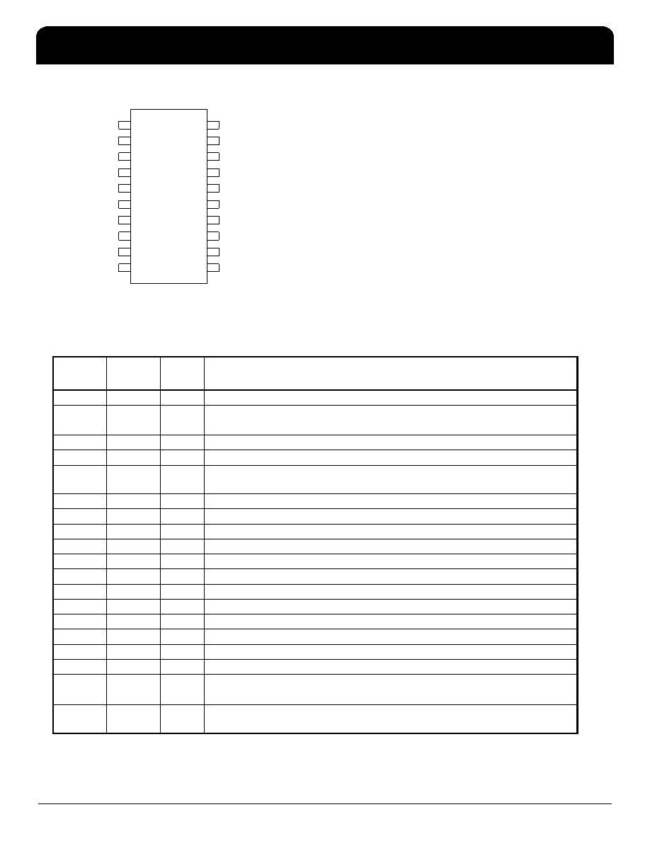
Pin Assignment
Pin Descriptions
13
4
12
5
11
ASC1
8
9
10
VDD
CLKC2
CLKA2
CCS
CLKB2
DC
17
16
CLKB1
3
X1/ICLK
VDD
CLKA1
18
REFOUT
1
ASC0
X2
BCS0
20
BCS1
19
14
2
7
GND
CLKC1
OE
GND
15
6
20-pin (150 mil) SSOP
Pin
Number
Pin
Name
Pin
Type
Pin Description
1
ACS0
Input
A clock select 0. Selects outputs on CLKA1 and CLKA2 per table on page 3.
2
X2
Input
Crystal connection. Connect to a fundamental crystal or leave unconnected for a clock
input.
3
X1/ICLK
Input
Crystal connection. Connect to a fundamental crystal or clock input.
4
VDD
Power
Connect to +3.3 V or 5 V. Must be the same as pin 16.
5
ACS1
Input
A clock select 1. Selects outputs on CLKA1 and CLKA2 per table on page 3. Internal
pull-up.
6
GND
Power
Connect to ground.
7
CLKC1
Output
Output Clock C1. Depends on setting of CCS per table on page 3.
8
CLKC2
Output
Output Clock C2. Depends on setting of CCS per table on page 3. Same as CLKC1.
9
CLKB2
Output
Output Clock B2. Depends on setting of BCS1, 0 per table on page 3.
10
CLKB1
Output
Output Clock B1. Depends on setting of BCS1, 0 per table on page 3.
11
CCS
Input
Clock C select pin. Selects outputs on CLKC1 and CLKC2 per table on page 3.
12
DC
-
Don’t connect. Do not connect anything to this pin.
13
CLKA2
Output
Output Clock A2. Depends on setting of ACS1, 0 per table on page 3.
14
GND
Power
Connect to ground.
15
OE
Input
Output enable. Tri-states all outputs when low. Internal pull-up.
16
VDD
Power
Connect to +3.3 V or 5 V. Must be the same as pin 4.
17
CLKA1
Output
Output Clock A1. Depends on setting of ACS1, 0 per table on page 3.
18
REFOUT
Output
Buffered reference clock output. Same frequency as crystal or clock input.
19
BCS0
Input
B clock select 0. Selects outputs on CLKB1 and CLKB2 per table on page 3.
20
BCS1
Input
B clock select 1. Selects outputs on CLKB1 and CLKB2 per table on page 3. Internal
pull-up.
相关PDF资料 |
PDF描述 |
|---|---|
| M83723/83G1624Y | CONN RCPT 24POS WALL MT W/PINS |
| M83723/83G1624N | CONN RCPT 24POS WALL MT W/PINS |
| MS3450W28-20P | CONN RCPT 14POS WALL MNT W/PINS |
| VI-24N-MY-F2 | CONVERTER MOD DC/DC 18.5V 50W |
| CY28419OCT | IC CLOCK SRC CK409B 56SSOP |
相关代理商/技术参数 |
参数描述 |
|---|---|
| ICS650R-27IT | 功能描述:IC CLK SOURCE NETWORK 20-SSOP RoHS:否 类别:集成电路 (IC) >> 时钟/计时 - 时钟发生器,PLL,频率合成器 系列:- 产品变化通告:Product Discontinuation 04/May/2011 标准包装:96 系列:- 类型:时钟倍频器,零延迟缓冲器 PLL:带旁路 输入:LVTTL 输出:LVTTL 电路数:1 比率 - 输入:输出:1:8 差分 - 输入:输出:无/无 频率 - 最大:133.3MHz 除法器/乘法器:是/无 电源电压:3 V ~ 3.6 V 工作温度:0°C ~ 70°C 安装类型:表面贴装 封装/外壳:16-TSSOP(0.173",4.40mm 宽) 供应商设备封装:16-TSSOP 包装:管件 其它名称:23S08-5HPGG |
| ICS651 | 制造商:ICS 制造商全称:ICS 功能描述:LOW SKEW 1 TO 4 CLOCK BUFFER |
| ICS65-1 | 制造商:Thomas & Betts 功能描述:INSULATED SERV.ENTR.SLEEVE 制造商:Thomas & Betts 功能描述:Cable Accessories Compression Splice Aluminum |
| ICS651-03 | 制造商:ICS 制造商全称:ICS 功能描述:VOIP Clock Source |
| ICS651B | 制造商:IDT 制造商全称:Integrated Device Technology 功能描述:LOW SKEW 1 TO 4 CLOCK BUFFER |
发布紧急采购,3分钟左右您将得到回复。