- 您现在的位置:买卖IC网 > PDF目录131796 > ICS673-01M PLL BASED CLOCK DRIVER, 2 TRUE OUTPUT(S), 0 INVERTED OUTPUT(S), PDSO16 PDF资料下载
参数资料
| 型号: | ICS673-01M |
| 元件分类: | 时钟及定时 |
| 英文描述: | PLL BASED CLOCK DRIVER, 2 TRUE OUTPUT(S), 0 INVERTED OUTPUT(S), PDSO16 |
| 封装: | 0.150 INCH, SOIC-16 |
| 文件页数: | 5/8页 |
| 文件大小: | 104K |
| 代理商: | ICS673-01M |
PLL BUILDING BLOCK
MDS 673-01 F
5
Revision 040102
Int egrat ed C i rcuit Syste ms q 525 R a ce S t r eet, San Jose, CA 95126 q t e l (40 8 ) 295 -9800 q
w w w. icst . c om
ICS673-01
ceramics have piezoelectric properties that convert
mechanical vibration into voltage noise that interferes
with VCXO operation.
For larger loop capacitor values such as 0.1
F or 1 F,
PPS film types made by Panasonic, or metal poly types
made by Murata or Cornell Dubilier are recommended.
For questions or changes regarding loop filter
characteristics, please contact your sales area FAE, or
ICS MicroClock Applications.
Avoiding PLL Lockup
In some applications, the ICS673-01 can “lock up” at
the maximum VCO frequency. This is usually caused
by power supply glitches or a very slow power supply
ramp. This situation also occurs if the external divider
starts to fall at high input frequencies. The usual failure
mode of a divider circuit is that the output of the divider
begins to miss clock edges. The phase detector
interprets this as a too low output frequency and
increases the VCO frequency. The feedback divider
begis to miss even more clock edges and the VCO
frequency is continually increased until it is running at
the maximum. Whether caused by power supply issues
or by the existing divider, the loop can only recover by
powering down the circuit, asserting PD, or shorterning
the loop filter to ground.
The simplest way to avoid this problem is to use an
external divider that always operates correctly
regardless of the VCO speed. Figures 2 and 3 show
that the VCO is capable of high speeds. By using the
internal divide-by-four and/or the CLK2 output, the
maximum VCO frequency can be divided by 2, 4, or 8
and a slower counter can be used. Using the ICS673
internal dividers in this manner does reduce the
number of frequencies that can be exactly synthesized
by forcing the total VCO divide to change in increments
of 2, 4, or 8.
If this lockup problem occurs, there are several
solutions; three of which are described below.
1. If the system has a reset or power good signal, this
should be applied to the PD pin, forcing the chip to stay
powered down until the power supply voltage has
stabilized
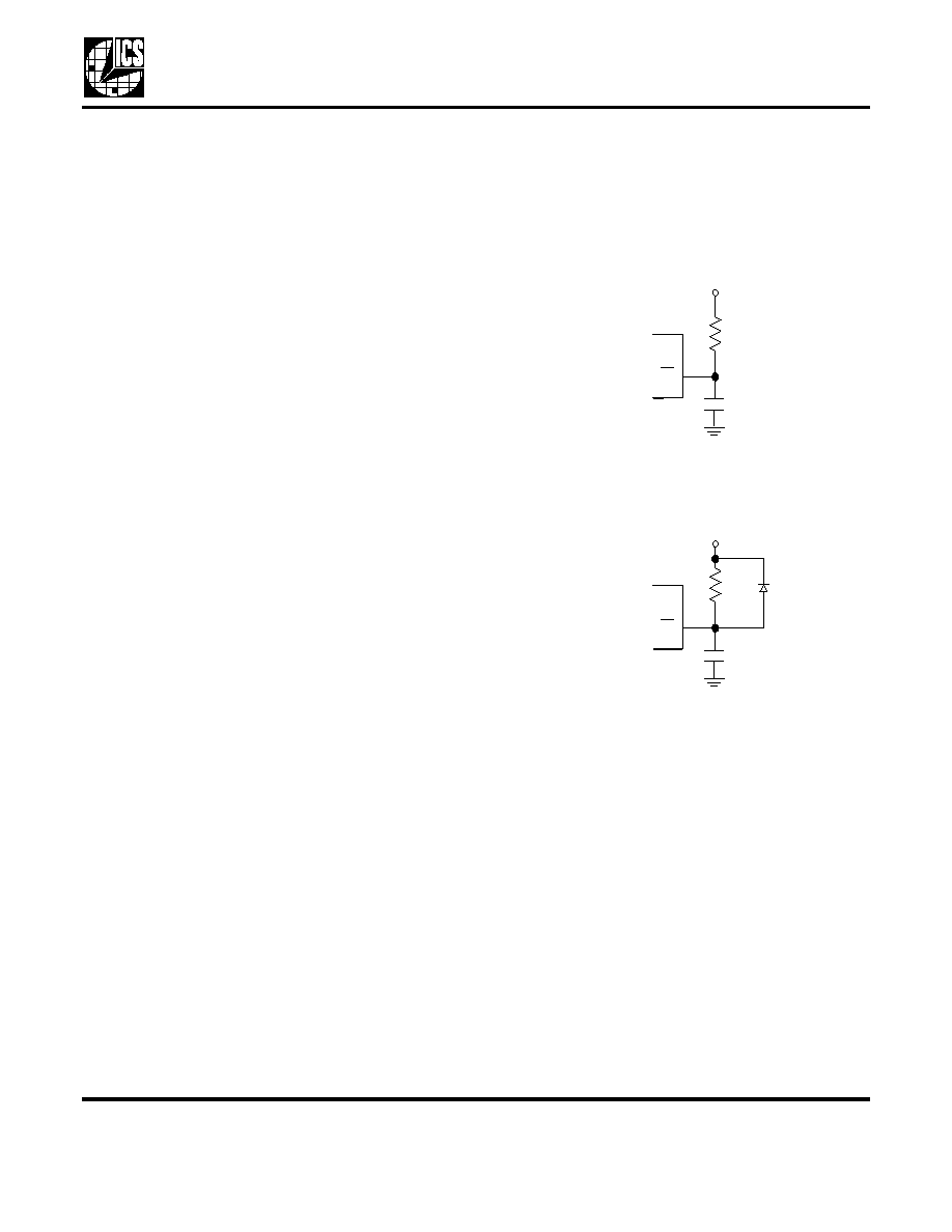
2. If no power good signal is available, a simple
power-on reset circuit can be attached to the PD pin, as
shown in Figure 4. When the power supply ramps up,
this circuit holds PD asserted (device powered down)
until the capacitor charges.
The circuit of Figure 4A is adequate in most cases, but
the discharge rate of capacitor C3 when VDD goes low
is limited by R1. As this discharge rate determines the
minimum reset time, the circuit of Figure 4B may be
used when a faster reset time is desired. The values of
R1 and C3 should be selected to ensure that PD stays
below 1.0 V until the power supply is stable.
3. A comparator circuit may be used to monitor the loop
filter voltage, as shown in Figure 5. This circuit will
dump the charge off the loop filter by asserting PD if the
VCO begins to run too fast and the PLL can recover. A
good choice for thie comparator is the National
Semiconductor LMC7211BIM5X. It is low power, ver
small (SOT-23), low cost, and has high input
impedance.
The trigger voltage of the comparator is set by the
voltage divider formed by R2 and R3. The voltage
A. Ba si c Ci r cui t
R
1
C
3
PD
I CS673 - 01
VDD
B. Fa st er Di sch ar g e
R
1
C
3
PD
I CS673 - 01
VDD
D
1
相关PDF资料 |
PDF描述 |
|---|---|
| IDTQS74FCT2374CTQ8 | FCT SERIES, 8-BIT DRIVER, TRUE OUTPUT, PDSO20 |
| IDT74LVCHR16646APV8 | LVC/LCX/Z SERIES, DUAL 8-BIT REGISTERED TRANSCEIVER, TRUE OUTPUT, PDSO56 |
| IDT74LVCHR16646APA8 | LVC/LCX/Z SERIES, DUAL 8-BIT REGISTERED TRANSCEIVER, TRUE OUTPUT, PDSO56 |
| ICS853011AM | LOW SKEW CLOCK DRIVER, 2 TRUE OUTPUT(S), 0 INVERTED OUTPUT(S), PDSO8 |
| ICS853011AMLF | LOW SKEW CLOCK DRIVER, 2 TRUE OUTPUT(S), 0 INVERTED OUTPUT(S), PDSO8 |
相关代理商/技术参数 |
参数描述 |
|---|---|
| ICS673M-01 | 功能描述:IC PLL BUILDING BLOCK 16-SOIC RoHS:否 类别:集成电路 (IC) >> 时钟/计时 - 时钟发生器,PLL,频率合成器 系列:- 产品变化通告:Product Discontinuation 04/May/2011 标准包装:96 系列:- 类型:时钟倍频器,零延迟缓冲器 PLL:带旁路 输入:LVTTL 输出:LVTTL 电路数:1 比率 - 输入:输出:1:8 差分 - 输入:输出:无/无 频率 - 最大:133.3MHz 除法器/乘法器:是/无 电源电压:3 V ~ 3.6 V 工作温度:0°C ~ 70°C 安装类型:表面贴装 封装/外壳:16-TSSOP(0.173",4.40mm 宽) 供应商设备封装:16-TSSOP 包装:管件 其它名称:23S08-5HPGG |
| ICS673M-01I | 功能描述:IC PLL BUILDING BLOCK 16-SOIC RoHS:否 类别:集成电路 (IC) >> 时钟/计时 - 时钟发生器,PLL,频率合成器 系列:- 产品变化通告:Product Discontinuation 04/May/2011 标准包装:96 系列:- 类型:时钟倍频器,零延迟缓冲器 PLL:带旁路 输入:LVTTL 输出:LVTTL 电路数:1 比率 - 输入:输出:1:8 差分 - 输入:输出:无/无 频率 - 最大:133.3MHz 除法器/乘法器:是/无 电源电压:3 V ~ 3.6 V 工作温度:0°C ~ 70°C 安装类型:表面贴装 封装/外壳:16-TSSOP(0.173",4.40mm 宽) 供应商设备封装:16-TSSOP 包装:管件 其它名称:23S08-5HPGG |
| ICS673M-01ILF | 功能描述:IC PLL BUILDING BLOCK 16SOIC RoHS:是 类别:集成电路 (IC) >> 时钟/计时 - 时钟发生器,PLL,频率合成器 系列:- 标准包装:1,000 系列:Precision Edge® 类型:时钟/频率合成器 PLL:无 输入:CML,PECL 输出:CML 电路数:1 比率 - 输入:输出:2:1 差分 - 输入:输出:是/是 频率 - 最大:10.7GHz 除法器/乘法器:无/无 电源电压:2.375 V ~ 3.6 V 工作温度:-40°C ~ 85°C 安装类型:表面贴装 封装/外壳:16-VFQFN 裸露焊盘,16-MLF? 供应商设备封装:16-MLF?(3x3) 包装:带卷 (TR) 其它名称:SY58052UMGTRSY58052UMGTR-ND |
| ICS673M-01ILFT | 功能描述:IC PLL BUILDING BLOCK 16-SOIC RoHS:是 类别:集成电路 (IC) >> 时钟/计时 - 时钟发生器,PLL,频率合成器 系列:- 标准包装:2,000 系列:- 类型:PLL 时钟发生器 PLL:带旁路 输入:LVCMOS,LVPECL 输出:LVCMOS 电路数:1 比率 - 输入:输出:2:11 差分 - 输入:输出:是/无 频率 - 最大:240MHz 除法器/乘法器:是/无 电源电压:3.135 V ~ 3.465 V 工作温度:0°C ~ 70°C 安装类型:表面贴装 封装/外壳:32-LQFP 供应商设备封装:32-TQFP(7x7) 包装:带卷 (TR) |
| ICS673M-01IT | 功能描述:IC PLL BUILDING BLOCK 16-SOIC RoHS:否 类别:集成电路 (IC) >> 时钟/计时 - 时钟发生器,PLL,频率合成器 系列:- 产品变化通告:Product Discontinuation 04/May/2011 标准包装:96 系列:- 类型:时钟倍频器,零延迟缓冲器 PLL:带旁路 输入:LVTTL 输出:LVTTL 电路数:1 比率 - 输入:输出:1:8 差分 - 输入:输出:无/无 频率 - 最大:133.3MHz 除法器/乘法器:是/无 电源电压:3 V ~ 3.6 V 工作温度:0°C ~ 70°C 安装类型:表面贴装 封装/外壳:16-TSSOP(0.173",4.40mm 宽) 供应商设备封装:16-TSSOP 包装:管件 其它名称:23S08-5HPGG |
发布紧急采购,3分钟左右您将得到回复。