- 您现在的位置:买卖IC网 > PDF目录9677 > ICS810001DK-21LF (IDT, Integrated Device Technology Inc)IC CLK GEN SYNC VCXO DL 32VFQFN PDF资料下载
参数资料
| 型号: | ICS810001DK-21LF |
| 厂商: | IDT, Integrated Device Technology Inc |
| 文件页数: | 4/19页 |
| 文件大小: | 0K |
| 描述: | IC CLK GEN SYNC VCXO DL 32VFQFN |
| 标准包装: | 490 |
| 系列: | HiPerClockS™, FemtoClock™ |
| 类型: | 时钟/频率发生器,转换器,抖动衰减器,多路复用器 |
| PLL: | 是 |
| 主要目的: | 视频 |
| 输入: | LVCMOS,LVTTL |
| 输出: | LVCMOS,LVTTL |
| 电路数: | 1 |
| 比率 - 输入:输出: | 2:1 |
| 差分 - 输入:输出: | 无/无 |
| 频率 - 最大: | 175MHz |
| 电源电压: | 3.135 V ~ 3.465 V |
| 工作温度: | 0°C ~ 70°C |
| 安装类型: | 表面贴装 |
| 封装/外壳: | 32-VFQFN 裸露焊盘 |
| 供应商设备封装: | 32-VFQFPN 裸露焊盘(4x4) |
| 包装: | 托盘 |
| 其它名称: | 800-2276 ICS810001DK-21LF-ND |
ICS810001DK-21 REVISION B APRIL 13, 2010
12
2010 Integrated Device Technology, Inc.
ICS810001-21 Data Sheet
FEMTOCLOCK DUAL VCXO VIDEO PLL
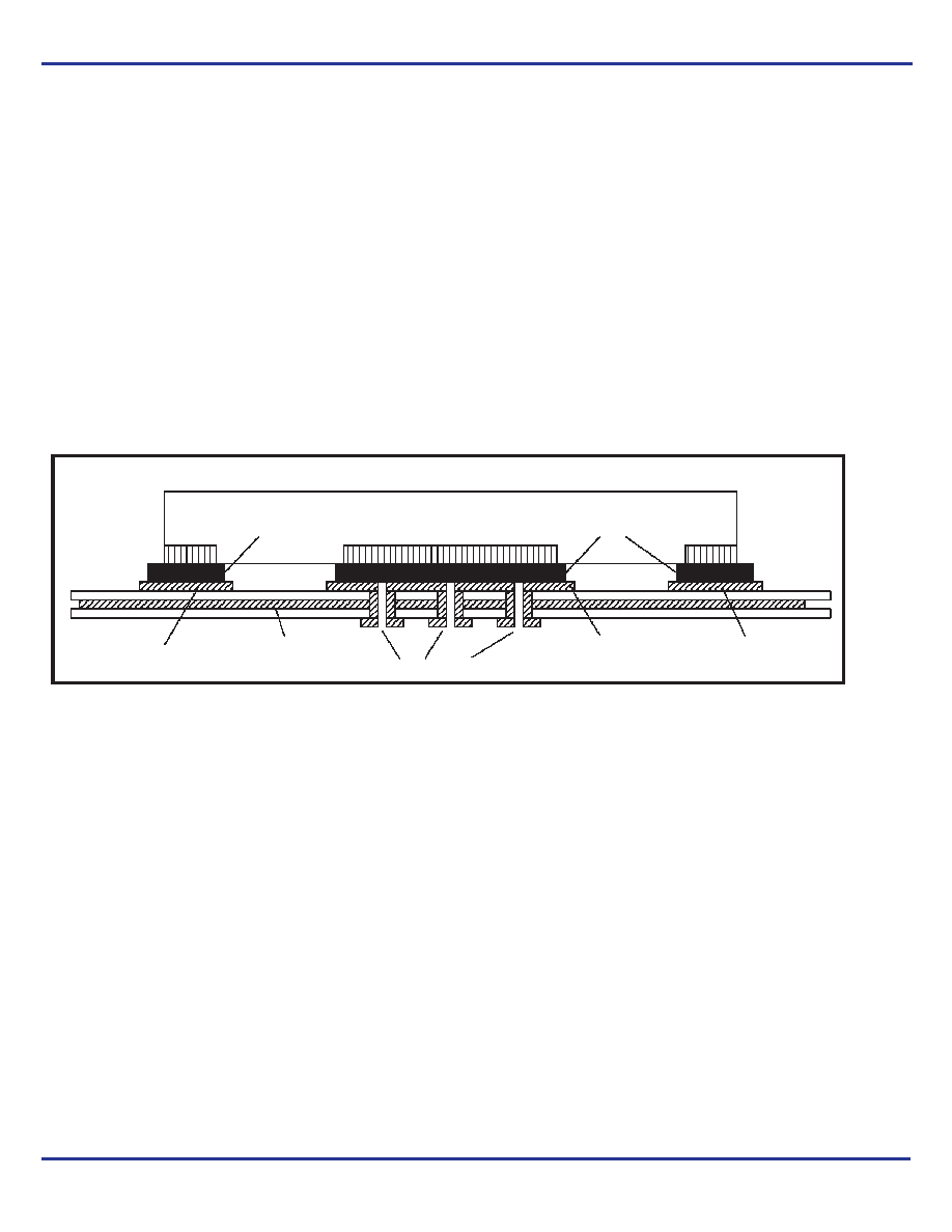
VFQFN EPAD Thermal Release Path
In order to maximize both the removal of heat from the package and
the electrical performance, a land pattern must be incorporated on
the Printed Circuit Board (PCB) within the footprint of the package
corresponding to the exposed metal pad or exposed heat slug on the
package, as shown in Figure 2. The solderable area on the PCB, as
defined by the solder mask, should be at least the same size/shape
as the exposed pad/slug area on the package to maximize the
thermal/electrical performance. Sufficient clearance should be
designed on the PCB between the outer edges of the land pattern
and the inner edges of pad pattern for the leads to avoid any shorts.
While the land pattern on the PCB provides a means of heat transfer
and electrical grounding from the package to the board through a
solder joint, thermal vias are necessary to effectively conduct from
the surface of the PCB to the ground plane(s). The land pattern must
be connected to ground through these vias. The vias act as “heat
pipes”. The number of vias (i.e. “heat pipes”) are application specific
and dependent upon the package power dissipation as well as
electrical conductivity requirements. Thus, thermal and electrical
analysis and/or testing are recommended to determine the minimum
number needed. Maximum thermal and electrical performance is
achieved when an array of vias is incorporated in the land pattern. It
is recommended to use as many vias connected to ground as
possible. It is also recommended that the via diameter should be 12
to 13mils (0.30 to 0.33mm) with 1oz copper via barrel plating. This is
desirable to avoid any solder wicking inside the via during the
soldering process which may result in voids in solder between the
exposed pad/slug and the thermal land. Precautions should be taken
to eliminate any solder voids between the exposed heat slug and the
land pattern. Note: These recommendations are to be used as a
guideline only. For further information, please refer to the Application
Note on the Surface Mount Assembly of Amkor’s
Thermally/Electrically Enhance Leadframe Base Package, Amkor
Technology.
Figure 2. P.C. Assembly for Exposed Pad Thermal Release Path – Side View (drawing not to scale)
SOLDER
PIN
EXPOSED HEAT SLUG
PIN PAD
GROUND PLANE
LAND PATTERN
(GROUND PAD)
THERMAL VIA
相关PDF资料 |
PDF描述 |
|---|---|
| VE-J4M-MX-F4 | CONVERTER MOD DC/DC 10V 75W |
| VE-J4M-MX-F3 | CONVERTER MOD DC/DC 10V 75W |
| VE-2V3-MX-F4 | CONVERTER MOD DC/DC 24V 75W |
| ICS874001AGI-05LF | IC PCI EXPRSS/JITT ATTEN 20TSSOP |
| MS27508E22B1S | CONN RCPT 100POS BOX MNT W/SCKT |
相关代理商/技术参数 |
参数描述 |
|---|---|
| ICS810001DK-21LFT | 功能描述:IC CLK GEN SYNC VCXO DL 32VFQFN RoHS:是 类别:集成电路 (IC) >> 时钟/计时 - 专用 系列:HiPerClockS™, FemtoClock™ 标准包装:1,500 系列:- 类型:时钟缓冲器/驱动器 PLL:是 主要目的:- 输入:- 输出:- 电路数:- 比率 - 输入:输出:- 差分 - 输入:输出:- 频率 - 最大:- 电源电压:3.3V 工作温度:0°C ~ 70°C 安装类型:表面贴装 封装/外壳:28-SSOP(0.209",5.30mm 宽) 供应商设备封装:28-SSOP 包装:带卷 (TR) 其它名称:93786AFT |
| ICS810-06 | 制造商:ICS 制造商全称:ICS 功能描述:VCXO-TO-6 LVCMOS OUTPUTS |
| ICS81006AK | 制造商:ICS 制造商全称:ICS 功能描述:VCXO-TO-6 LVCMOS OUTPUTS |
| ICS81006AKI | 制造商:ICS 制造商全称:ICS 功能描述:VCXO-TO-6 LVCMOS OUTPUTS |
| ICS81006AKILF | 功能描述:IC VCXO TO 6 LVCMOS OUT 20VFQFPN RoHS:是 类别:集成电路 (IC) >> 时钟/计时 - 时钟发生器,PLL,频率合成器 系列:HiPerClockS™ 标准包装:1,000 系列:- 类型:时钟/频率合成器,扇出分配 PLL:- 输入:- 输出:- 电路数:- 比率 - 输入:输出:- 差分 - 输入:输出:- 频率 - 最大:- 除法器/乘法器:- 电源电压:- 工作温度:- 安装类型:表面贴装 封装/外壳:56-VFQFN 裸露焊盘 供应商设备封装:56-VFQFP-EP(8x8) 包装:带卷 (TR) 其它名称:844S012AKI-01LFT |
发布紧急采购,3分钟左右您将得到回复。