- 您现在的位置:买卖IC网 > PDF目录9578 > ICS841S012DKILFT (IDT, Integrated Device Technology Inc)IC FREQ SYNTHESIZER 56VFQFN PDF资料下载
参数资料
| 型号: | ICS841S012DKILFT |
| 厂商: | IDT, Integrated Device Technology Inc |
| 文件页数: | 2/23页 |
| 文件大小: | 0K |
| 描述: | IC FREQ SYNTHESIZER 56VFQFN |
| 标准包装: | 1,000 |
| 系列: | HiPerClockS™, PCI Express® (PCIe) |
| 类型: | 时钟/频率合成器,多路复用器 |
| PLL: | 是 |
| 主要目的: | PCI Express(PCIe) |
| 输入: | LVCMOS,LVTTL,晶体 |
| 输出: | HCSL,LVCMOS,LVTTL |
| 电路数: | 1 |
| 比率 - 输入:输出: | 2:12 |
| 差分 - 输入:输出: | 是/无 |
| 频率 - 最大: | 250MHz |
| 电源电压: | 3.135 V ~ 3.465 V |
| 工作温度: | -40°C ~ 85°C |
| 安装类型: | 表面贴装 |
| 封装/外壳: | 56-VFQFN 裸露焊盘 |
| 供应商设备封装: | 56-VFQFP-EP(8x8) |
| 包装: | 带卷 (TR) |
ICS841S012BKI REVISION A NOVEMBER 10, 2009
10
2009 Integrated Device Technology, Inc.
ICS841S012I Data Sheet
CRYSTAL-TO-0.7V DIFFERENTIAL HCSL/LVCMOS FREQUENCY SYNTHESIZER
APPLICATION INFORMATION
As in any high speed analog circuitry, the power supply pins are
vulnerable to random noise. To achieve optimum jitter perfor-
mance, power supply isolation is required. The ICS841S012I pro-
vides separate power supplies to isolate any high switching noise
from the outputs to the internal PLL. V
DD, VDDA, VDDOB, and VDDOC
should be individually connected to the power supply
plane through vias, and 0.01F bypass capacitors should be used
for each pin.
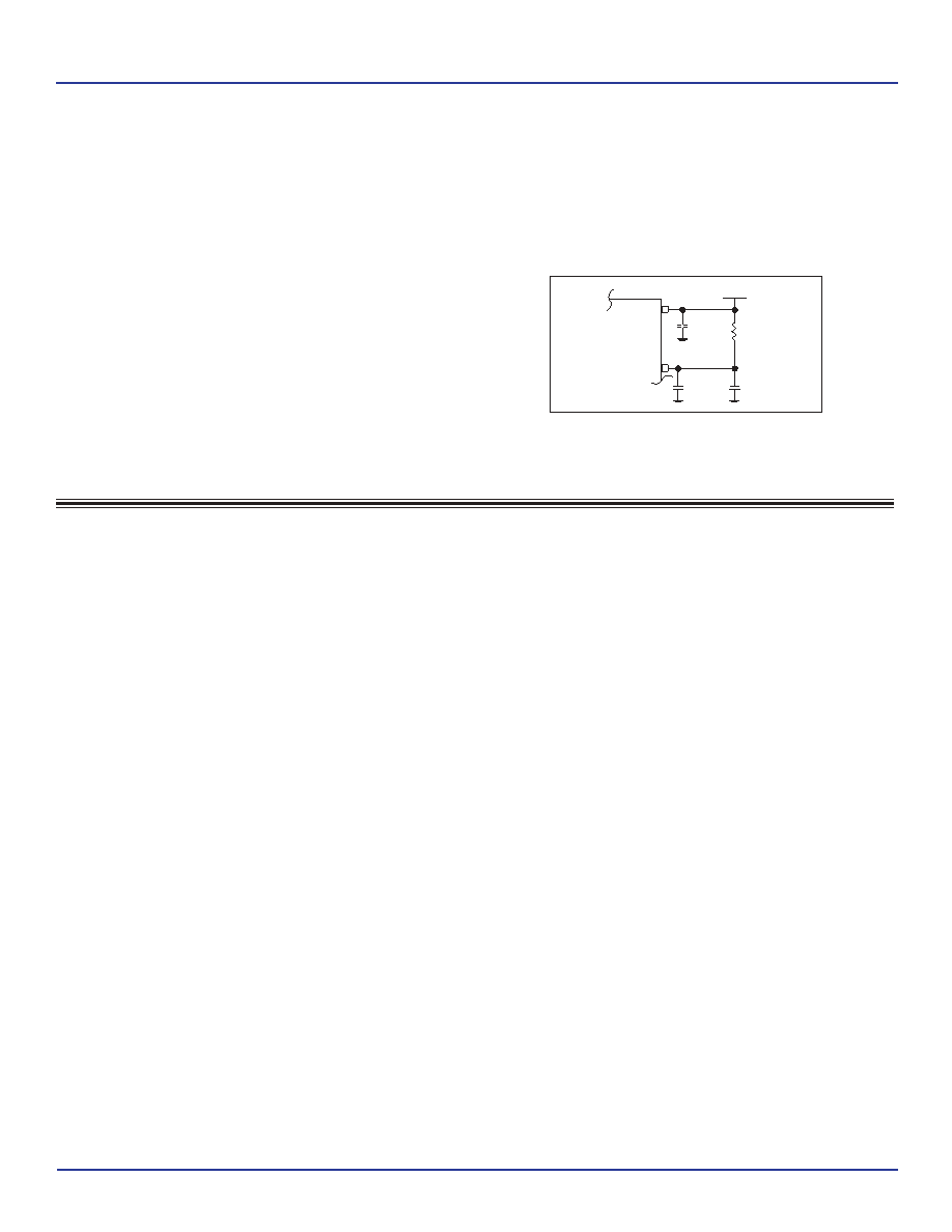
Figure 1 illustrates this for a generic V
DD pin and
also shows that V
DDA requires that an additional10Ω resistor
along with a 10F bypass capacitor be connected to the V
DDA pin.
The 10
Ω resistor can also be replaced by a ferrite bead.
POWER SUPPLY FILTERING TECHNIQUES
FIGURE 1. POWER SUPPLY FILTERING
10
Ω
V
DDA
10
μF
.01
μF
3.3V
.01
μF
V
DD
INPUTS:
CRYSTAL INPUTS
For applications not requiring the use of the crystal oscillator
input, both XTAL_IN and XTAL_OUT can be left floating. Though
not required, but for additional protection, a 1k
Ω resistor can be
tied from XTAL_IN to ground.
REF_IN INPUT
For applications not requiring the use of the reference clock,
it can be left floating. Though not required, but for additional
protection, a 1k
Ω resistor can be tied from the REF_IN to ground.
LVCMOS CONTROL PINS
All control pins have internal pull-ups or pull-downs; additional
resistance is not required but can be added for additional
protection. A 1k
Ω resistor can be used.
RECOMMENDATIONS FOR UNUSED INPUT AND OUTPUT PINS
OUTPUTS:
LVCMOS OUTPUTS
All unused LVCMOS output can be left floating. We recommend
that there is no trace attached.
DIFFERENTIAL OUTPUT
All unused differential outputs can be left floating. We recommend
that there is no trace attached. Both sides of the differential output
pair should either be left floating or terminated.
相关PDF资料 |
PDF描述 |
|---|---|
| VE-BN0-MY-S | CONVERTER MOD DC/DC 5V 50W |
| VE-BN0-IU | CONVERTER MOD DC/DC 5V 200W |
| VE-B1L-MW-F2 | CONVERTER MOD DC/DC 28V 100W |
| VE-B1K-MW-F4 | CONVERTER MOD DC/DC 40V 100W |
| VE-B1J-MW-F2 | CONVERTER MOD DC/DC 36V 100W |
相关代理商/技术参数 |
参数描述 |
|---|---|
| ICS841S012I | 制造商:IDT 制造商全称:Integrated Device Technology 功能描述:Crystal-to-0.7V Differential HCSL/LVCMOS Frequency Synthesizer |
| ICS841S01BG | 制造商:IDT 制造商全称:Integrated Device Technology 功能描述:PCI EXPRESS⑩ CLOCK GENERATOR |
| ICS841S01BGLF | 功能描述:IC CLK GENERATOR PLL 16-TSSOP RoHS:是 类别:集成电路 (IC) >> 时钟/计时 - 专用 系列:HiPerClockS™, PCI Express® (PCIe) 标准包装:1 系列:- 类型:时钟/频率发生器,多路复用器 PLL:是 主要目的:存储器,RDRAM 输入:晶体 输出:LVCMOS 电路数:1 比率 - 输入:输出:1:2 差分 - 输入:输出:无/是 频率 - 最大:400MHz 电源电压:3 V ~ 3.6 V 工作温度:0°C ~ 85°C 安装类型:表面贴装 封装/外壳:16-TSSOP(0.173",4.40mm 宽) 供应商设备封装:16-TSSOP 包装:Digi-Reel® 其它名称:296-6719-6 |
| ICS841S01BGLFT | 制造商:IDT 制造商全称:Integrated Device Technology 功能描述:PCI EXPRESS⑩ CLOCK GENERATOR |
| ICS841S01BGT | 制造商:IDT 制造商全称:Integrated Device Technology 功能描述:PCI EXPRESS⑩ CLOCK GENERATOR |
发布紧急采购,3分钟左右您将得到回复。