- 您现在的位置:买卖IC网 > PDF目录67689 > ICS8430BYI-71 (INTEGRATED DEVICE TECHNOLOGY INC) 700 MHz, OTHER CLOCK GENERATOR, PQFP32 PDF资料下载
参数资料
| 型号: | ICS8430BYI-71 |
| 厂商: | INTEGRATED DEVICE TECHNOLOGY INC |
| 元件分类: | 时钟产生/分配 |
| 英文描述: | 700 MHz, OTHER CLOCK GENERATOR, PQFP32 |
| 封装: | 7 X 7 MM, 1.40 MM HEIGHT, MS-026BBA, LQFP-32 |
| 文件页数: | 9/16页 |
| 文件大小: | 167K |
| 代理商: | ICS8430BYI-71 |
8430BYI-71
www.icst.com/products/hiperclocks.html
REV. A FEBRUARY 17, 2006
2
Integrated
Circuit
Systems, Inc.
ICS8430BI-71
700MHZ, LOW JITTER, CRYSTAL INTERFACE/
LVCMOS-TO-3.3V LVPECL FREQUENCY SYNTHESIZER
PRELIMINARY
specific default state that will automatically occur during
power-up. The TEST output is LOW when operating in the
parallel input mode. The relationship between the VCO fre-
quency, the crystal frequency and the M divider is defined as
follows:
The M value and the required values of M0 through M8 are
shown in Table 3B, Programmable VCO Frequency Function
Table. Valid M values for which the PLL will achieve lock for a
16MHz reference are defined as 125
≤ M ≤ 350.The frequency
out is defined as follows:
Serial operation occurs when nP_LOAD is HIGH and S_LOAD
is LOW. The shift register is loaded by sampling the S_DATA
bits with the rising edge of S_CLOCK. The contents of the
shift register are loaded into the M divider and N output di-
vider when S_LOAD transitions from LOW-to-HIGH. The M
divide and N output divide values are latched on the HIGH-
to-LOW transition of S_LOAD. If S_LOAD is held HIGH, data
at the S_DATA input is passed directly to the M divider and N
output divider on each rising edge of S_CLOCK. The serial
mode can be used to program the M and N bits and test bits
T1 and T0. The internal registers T0 and T1 determine the state
of the TEST output as follows:
NOTE: The functional description that follows describes op-
eration using a 16MHz crystal. Valid PLL loop divider values
for different crystal or input frequencies are defined in the In-
put Frequency Characteristics, Table 5, NOTE 1.
The ICS8430BI-71 features a fully integrated PLL and there-
fore requires no external components for setting the loop band-
width. A parallel-resonant, fundamental crystal is used as the
input to the on-chip oscillator. The output of the oscillator is
divided by 16 prior to the phase detector. With a 16MHz crys-
tal, this provides a 1MHz reference frequency. The VCO of
the PLL operates over a range of 250MHz to 700MHz. The
output of the M divider is also applied to the phase detector.
The phase detector and the M divider force the VCO output
frequency to be 2M times the reference frequency by adjust-
ing the VCO control voltage. Note that for some values of M
(either too high or too low), the PLL will not achieve lock. The
output of the VCO is scaled by a divider prior to being sent to
each of the LVPECL output buffers. The divider provides a
50% output duty cycle.
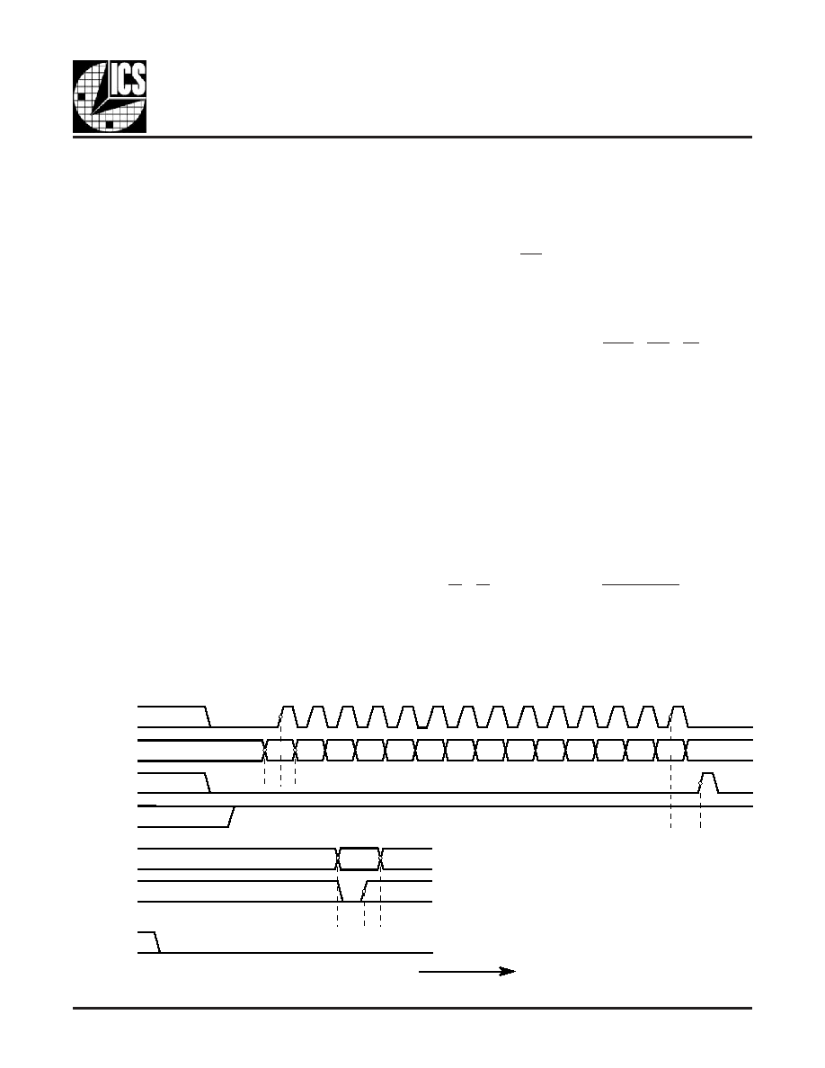
The programmable features of the ICS8430BI-71 support two
input modes to program the M divider and N output divider.
The two input operational modes are parallel and serial. Fig-
ure 1 shows the timing diagram for each mode. In parallel
mode, the nP_LOAD input is initially LOW. The data on inputs
M0 through M8 and N0 through N2 is passed directly to the M
divider and N output divider. On the LOW-to-HIGH transition
of the nP_LOAD input, the data is latched and the M divider
remains loaded until the next LOW transition on nP_LOAD or
until a serial event occurs. As a result, the M and N bits can
be hardwired to set the M divider and N output divider to a
FUNCTIONAL DESCRIPTION
N
fout = fVCO =
16
2M
fxtal x
N
16
fVCO =
fxtal x 2M
T1
T0
TEST Output
0
LOW
0
1
S_Data clocked into register
1
0
Output of M divider
1
CMOS Fout
FIGURE 1. PARALLEL & SERIAL LOAD OPERATIONS
Time
SERIAL LOADING
PARALLEL LOADING
t
S
t
H
t
S
t
H
t
S
M, N
T1
T0
N2
N1
N0
M8
M7
M6
M5
M4
M3
M2
M1
M0
S_CLOCK
S_DATA
S_LOAD
nP_LOAD
M0:M8, N0:N2
nP_LOAD
S_LOAD
相关PDF资料 |
PDF描述 |
|---|---|
| ICS8430BYI-71T | 700 MHz, OTHER CLOCK GENERATOR, PQFP32 |
| ICS8430DY-01T | 500 MHz, OTHER CLOCK GENERATOR, PQFP32 |
| ICS8430DY-111LF | 8430 SERIES, PLL BASED CLOCK DRIVER, 2 TRUE OUTPUT(S), 0 INVERTED OUTPUT(S), PQFP32 |
| ICS8430DY-111T | 8430 SERIES, PLL BASED CLOCK DRIVER, 2 TRUE OUTPUT(S), 0 INVERTED OUTPUT(S), PQFP32 |
| ICS8430DY-111LFT | 8430 SERIES, PLL BASED CLOCK DRIVER, 2 TRUE OUTPUT(S), 0 INVERTED OUTPUT(S), PQFP32 |
相关代理商/技术参数 |
参数描述 |
|---|---|
| ICS8430BYI-71LF | 功能描述:IC SYNTHESIZER DUAL 32-LQFP RoHS:是 类别:集成电路 (IC) >> 时钟/计时 - 时钟发生器,PLL,频率合成器 系列:HiPerClockS™ 标准包装:2,000 系列:- 类型:PLL 频率合成器 PLL:是 输入:晶体 输出:时钟 电路数:1 比率 - 输入:输出:1:1 差分 - 输入:输出:无/无 频率 - 最大:1GHz 除法器/乘法器:是/无 电源电压:4.5 V ~ 5.5 V 工作温度:-20°C ~ 85°C 安装类型:表面贴装 封装/外壳:16-LSSOP(0.175",4.40mm 宽) 供应商设备封装:16-SSOP 包装:带卷 (TR) 其它名称:NJW1504V-TE1-NDNJW1504V-TE1TR |
| ICS8430BYI-71LFT | 功能描述:IC SYNTHESIZER DUAL 32-LQFP RoHS:是 类别:集成电路 (IC) >> 时钟/计时 - 时钟发生器,PLL,频率合成器 系列:HiPerClockS™ 标准包装:1,000 系列:- 类型:时钟/频率合成器,扇出分配 PLL:- 输入:- 输出:- 电路数:- 比率 - 输入:输出:- 差分 - 输入:输出:- 频率 - 最大:- 除法器/乘法器:- 电源电压:- 工作温度:- 安装类型:表面贴装 封装/外壳:56-VFQFN 裸露焊盘 供应商设备封装:56-VFQFP-EP(8x8) 包装:带卷 (TR) 其它名称:844S012AKI-01LFT |
| ICS8430BYI-71T | 制造商:ICS 制造商全称:ICS 功能描述:700MHZ, LOW JITTER, CRYSTAL INTERFACE / LVCMOS-TO-3.3V LVPECL FREQUENCY SYNTHESIZER |
| ICS8430CY-11T | 制造商:ICS 制造商全称:ICS 功能描述:700MHZ/350MHZ, LOW PHASE NOISE, CRYSTAL-TO- 3.3V LVPECL FREQUENCY SYNTHESIZER |
| ICS8430DY-111 | 制造商:ICS 制造商全称:ICS 功能描述:700MHZ, LOW JITTER DIFFERENTIAL-TO-3.3V LVPECL FREQUENCY SYNTHESIZER |
发布紧急采购,3分钟左右您将得到回复。