- 您现在的位置:买卖IC网 > PDF目录67690 > ICS8431EM-11 255 MHz, OTHER CLOCK GENERATOR, PDSO28 PDF资料下载
参数资料
| 型号: | ICS8431EM-11 |
| 元件分类: | 时钟产生/分配 |
| 英文描述: | 255 MHz, OTHER CLOCK GENERATOR, PDSO28 |
| 封装: | 7.50 X 18.05 MM, 2.25 MM HEIGHT, MS-013, MO-119, SOIC-28 |
| 文件页数: | 2/17页 |
| 文件大小: | 561K |
| 代理商: | ICS8431EM-11 |
8431EM-11
www.icst.com/products/hiperclocks.html
REV. D OCTOBER 21, 2004
10
Integrated
Circuit
Systems, Inc.
ICS8431-11
255MHZ, LOW JITTER, CRYSTAL OSCILLATOR-
TO
-3.3V LVPECL FREQUENCY SYNTHESIZER
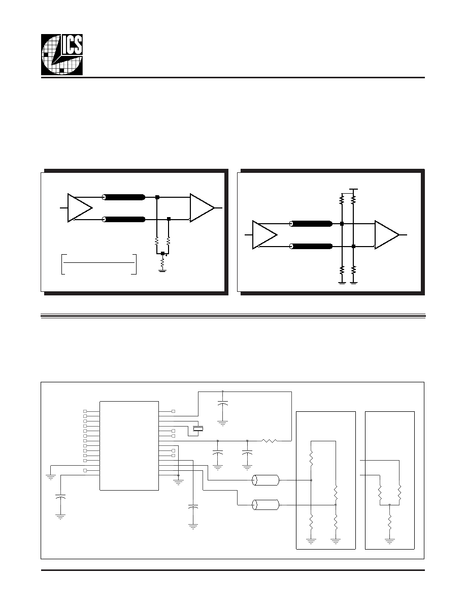
The clock layout topology shown below is typical for
IA64/32 platforms. The two different layouts mentioned are
recommended only as guidelines.
FOUT and nFOUT are low impedance follower outputs that
generate ECL/LVPECL compatible outputs.Therefore, terminat-
ing resistors (DC current path to ground) or current sources
must be used for functionality. These outputs are designed to
FIGURE 4B. LVPECL OUTPUT TERMINATION
3.3V
125
125
84
84
Z
o = 50
Z
o = 50
FOUT
FIN
FIGURE 4A. LVPECL OUTPUT TERMINATION
V
CC - 2V
50
50
RTT
Z
o = 50
Z
o = 50
FOUT
FIN
RTT =
Z
o
1
((V
OH + VOL) / (VCC – 2)) – 2
V
CC-2V
FIGURE 5A. RECOMMENDED SCHEMATIC LAYOUT
drive 50
transmission lines. Matched impedance techniques
should be used to maximize operating frequency and minimize
signal distortion.
Figures 4A and 4B show two different layouts
which are recommended only as guidelines. Other suitable clock
layouts may exist and it would be recommended that the board
designers simulate to guarantee compatibility across all printed
circuit and clock component process variations.
The schematic of the ICS8431-11 layout example used in this
layout guideline is shown in
Figure 5A. The ICS8431-11 rec-
ommended PCB board layout for this example is shown in
Figure 5B. This layout example is used as a general guide-
VCC
C4
10uF
IN-
R1
50
VCCA
R1
125
C1
0.1uF
IN+
R2
84
VCC0
C6
0.01uF
TL1
Zo = 50 Ohm
VCC
U1
8431-11
1
2
3
4
5
6
7
8
9
10
11
12
13
14
15
16
17
18
19
20
21
22
23
24
28
27
26
25
M0
M1
M2
M3
M4
M5
M6
M7
M8
SSC_CTL0
SSC_CTL1
VEE
TEST_IO
VCC
VEE
nFOUT
FOUT
VCCO
NC
MR
VEE
VCCA
NC
nP_LOAD
VCC
XTAL1
XTAL2
Termination
B (not shown
in the layout)
R3
50
C3
0.01uF
R5
10
IN+
TL2
Zo = 50 Ohm
C2
0.1uF
X1
R3
125
Termination A
R2
50
IN-
R4
84
LAYOUT GUIDELINE
TERMINATION FOR LVPECL OUTPUTS
line. The layout in the actual system will depend on the se-
lected component types, the density of the components, the
density of the traces, and the stack up of the P.C. board.
相关PDF资料 |
PDF描述 |
|---|---|
| ICS8431EMI-01 | 200 MHz, OTHER CLOCK GENERATOR, PDSO28 |
| ICS843201AG-375LF | 375 MHz, OTHER CLOCK GENERATOR, PDSO16 |
| ICS843201AG-375T | 375 MHz, OTHER CLOCK GENERATOR, PDSO16 |
| ICS843201AG-375 | 375 MHz, OTHER CLOCK GENERATOR, PDSO16 |
| ICS843204AGI | 156.25 MHz, OTHER CLOCK GENERATOR, PDSO48 |
相关代理商/技术参数 |
参数描述 |
|---|---|
| ICS8431I-21 | 制造商:ICS 制造商全称:ICS 功能描述:350MHZ, LOW JITTER, CRYSTAL OSCILLATOR-TO-3.3V LVPECL FREQUENCY SYNTHESIZER |
| ICS84320-01 | 制造商:IDT 制造商全称:Integrated Device Technology 功能描述:780MHZ, CRYSTAL-TO-3.3V DIFFERENTIAL LVPECL FREQUENCY SYNTHESIZER |
| ICS84320-01K | 制造商:ICS 制造商全称:ICS 功能描述:780MHZ, CRYSTAL-TO-3.3V DIFFERENTIAL LVPECL FREQUENCY SYNTHESIZER |
| ICS843201AG-375LF | 功能描述:IC SYNTHESIZER 375MHZ 16-TSSOP RoHS:是 类别:集成电路 (IC) >> 时钟/计时 - 时钟发生器,PLL,频率合成器 系列:HiPerClockS™, FemtoClock™ 标准包装:27 系列:Precision Edge® 类型:频率合成器 PLL:是 输入:PECL,晶体 输出:PECL 电路数:1 比率 - 输入:输出:1:1 差分 - 输入:输出:无/是 频率 - 最大:800MHz 除法器/乘法器:是/无 电源电压:3.135 V ~ 5.25 V 工作温度:0°C ~ 85°C 安装类型:表面贴装 封装/外壳:28-SOIC(0.295",7.50mm 宽) 供应商设备封装:28-SOIC 包装:管件 |
| ICS843201AG-375LFT | 功能描述:IC SYNTHESIZER 375MHZ 16-TSSOP RoHS:是 类别:集成电路 (IC) >> 时钟/计时 - 时钟发生器,PLL,频率合成器 系列:HiPerClockS™, FemtoClock™ 标准包装:27 系列:Precision Edge® 类型:频率合成器 PLL:是 输入:PECL,晶体 输出:PECL 电路数:1 比率 - 输入:输出:1:1 差分 - 输入:输出:无/是 频率 - 最大:800MHz 除法器/乘法器:是/无 电源电压:3.135 V ~ 5.25 V 工作温度:0°C ~ 85°C 安装类型:表面贴装 封装/外壳:28-SOIC(0.295",7.50mm 宽) 供应商设备封装:28-SOIC 包装:管件 |
发布紧急采购,3分钟左右您将得到回复。