- 您现在的位置:买卖IC网 > PDF目录67691 > ICS8432DYI-101LFT 8432 SERIES, PLL BASED CLOCK DRIVER, 2 TRUE OUTPUT(S), 0 INVERTED OUTPUT(S), PQFP32 PDF资料下载
参数资料
| 型号: | ICS8432DYI-101LFT |
| 元件分类: | 时钟及定时 |
| 英文描述: | 8432 SERIES, PLL BASED CLOCK DRIVER, 2 TRUE OUTPUT(S), 0 INVERTED OUTPUT(S), PQFP32 |
| 封装: | 7 X 7 MM, 1.40 MM HEIGHT, ROHS COMPLIANT, MS-026, LQFP-32 |
| 文件页数: | 18/18页 |
| 文件大小: | 173K |
| 代理商: | ICS8432DYI-101LFT |
8432DYI-101
www.icst.com/products/hiperclocks.html
REV. A MAY 23, 2005
9
Integrated
Circuit
Systems, Inc.
ICS8432I-101
700MHZ,
DIFFERENTIAL-TO-3.3V LVPECL FREQUENCY SYNTHESIZER
V
CC - 2V
50
Ω
50
Ω
RTT
Z
o = 50Ω
Z
o = 50Ω
FOUT
FIN
RTT =
Z
o
1
((V
OH + VOL) / (VCC – 2)) – 2
3.3V
125
Ω
125
Ω
84
Ω
84
Ω
Z
o = 50Ω
Z
o = 50Ω
FOUT
FIN
The clock layout topology shown below is a typical termina-
tion for LVPECL outputs. The two different layouts mentioned
are recommended only as guidelines.
FOUT and nFOUT are low impedance follower outputs that
generate ECL/LVPECL compatible outputs. Therefore, termi-
nating resistors (DC current path to ground) or current
sources must be used for functionality. These outputs are
FIGURE 4B. LVPECL OUTPUT TERMINATION
FIGURE 4A. LVPECL OUTPUT TERMINATION
designed to drive 50
Ω transmission lines. Matched impedance
techniques should be used to maximize operating frequency
and minimize signal distortion.
Figures 4A and 4B show two
different layouts which are recommended only as guidelines.
Other suitable clock layouts may exist and it would be rec-
ommended that the board designers simulate to guarantee
compatibility across all printed circuit and clock component
process variations.
TERMINATION FOR LVPECL OUTPUTS
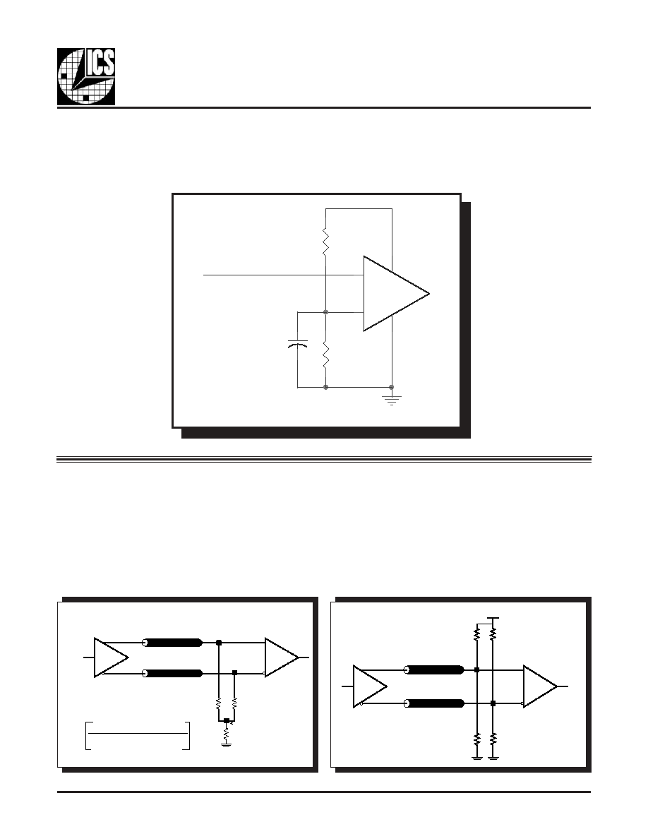
Figure 3 shows how the differential input can be wired to accept
single ended levels. The reference voltage V_REF = V
CC/2 is
generated by the bias resistors R1, R2 and C1.This bias circuit
should be located as close as possible to the input pin.The ratio
FIGURE 3. SINGLE ENDED SIGNAL DRIVING DIFFERENTIAL INPUT
WIRING THE DIFFERENTIAL INPUT TO ACCEPT SINGLE ENDED LEVELS
of R1 and R2 might need to be adjusted to position the V_REF in
the center of the input voltage swing. For example, if the input
clock swing is only 2.5V and V
CC = 3.3V, V_REF should be 1.25V
and R2/R1 = 0.609.
V_REF
R1
1K
C1
0.1u
R2
1K
Single Ended Clock Input
CLK
nCLK
VCC
相关PDF资料 |
PDF描述 |
|---|---|
| ICS8432DYI-101LF | 8432 SERIES, PLL BASED CLOCK DRIVER, 2 TRUE OUTPUT(S), 0 INVERTED OUTPUT(S), PQFP32 |
| ICS8432DYI-101T | 8432 SERIES, PLL BASED CLOCK DRIVER, 2 TRUE OUTPUT(S), 0 INVERTED OUTPUT(S), PQFP32 |
| ICS84330AM-01 | 700 MHz, OTHER CLOCK GENERATOR, PDSO28 |
| ICS84330AM-01LF | 700 MHz, OTHER CLOCK GENERATOR, PDSO28 |
| ICS84330AVLF | 700 MHz, OTHER CLOCK GENERATOR, PQCC28 |
相关代理商/技术参数 |
参数描述 |
|---|---|
| ICS8432DYI-101T | 制造商:ICS 制造商全称:ICS 功能描述:700MHZ, DIFFERENTIAL-TO-3.3V LVPECL FREQUENCY SYNTHESIZER |
| ICS8432I-101 | 制造商:ICS 制造商全称:ICS 功能描述:700MHZ, DIFFERENTIAL-TO-3.3V LVPECL FREQUENCY SYNTHESIZER |
| ICS8432I-51 | 制造商:IDT 制造商全称:Integrated Device Technology 功能描述:700MHZ, CYRSTAL-TO-3.3V DIFFERENTIAL LVPECL FREQUENCY SYNTHESIZER |
| ICS84330 | 制造商:ICS 制造商全称:ICS 功能描述:700MHZ, LOW JITTER, CRYSTAL-TO-3.3V DIFFERENTIAL LVPECL FREQUENCY SYNTHESIZER |
| ICS84330-01 | 制造商:ICS 制造商全称:ICS 功能描述:700MHZ, LOW JITTER, CRYSTAL-TO-3.3V DIFFERENTIAL LVPECL FREQUENCY SYNTHESIZER |
发布紧急采购,3分钟左右您将得到回复。