- 您现在的位置:买卖IC网 > PDF目录2073 > ICS85104AGILFT (IDT, Integrated Device Technology Inc)IC CLOCK BUFFER MUX 2:4 20-TSSOP PDF资料下载
参数资料
| 型号: | ICS85104AGILFT |
| 厂商: | IDT, Integrated Device Technology Inc |
| 文件页数: | 17/17页 |
| 文件大小: | 0K |
| 描述: | IC CLOCK BUFFER MUX 2:4 20-TSSOP |
| 产品培训模块: | PCI-Express |
| 标准包装: | 2,500 |
| 系列: | HiPerClockS™ |
| 类型: | 扇出缓冲器(分配),多路复用器 |
| 电路数: | 1 |
| 比率 - 输入:输出: | 2:4 |
| 差分 - 输入:输出: | 是/是 |
| 输入: | HCSL,LVCMOS,LVDS,LVHSTL,LVPECL,LVTTL,SSTL |
| 输出: | HCSL |
| 频率 - 最大: | 500MHz |
| 电源电压: | 2.97 V ~ 3.63 V |
| 工作温度: | -40°C ~ 85°C |
| 安装类型: | 表面贴装 |
| 封装/外壳: | 20-TSSOP(0.173",4.40mm 宽) |
| 供应商设备封装: | 20-TSSOP |
| 包装: | 带卷 (TR) |
| 其它名称: | 85104AGILFT |
ICS85104AGI REVISION A MAY 27, 2011
9
2011 Integrated Device Technology, Inc.
ICS85104I Data Sheet
LOW SKEW, 1-TO-4, DIFFERENTIAL/LVCMOS-TO-0.7V HCSL FANOUT BUFFER
APPLICATIONS INFORMATION
INPUTS:
CLK INPUT
For applications not requiring the use of a clock input, it can be
left floating. Though not required, but for additional protection, a
1k
Ω resistor can be tied from the CLK input to ground.
CLK/nCLK INPUTS
For applications not requiring the use of the differential input, both
CLK and nCLK can be left floating. Though not required, but for
additional protection, a 1k
Ω resistor can be tied from CLK to
ground.
LVCMOS CONTROL PINS
All control pins have internal pull-ups or pull-downs; additional
resistance is not required but can be added for additional
protection. A 1k
Ω resistor can be used.
RECOMMENDATIONS FOR UNUSED INPUT AND OUTPUT PINS
OUTPUTS:
DIFFERENTIAL OUTPUTs
All unused differential outputs can be left floating. We recommend
that there is no trace attached. Both sides of the differential output
pair should either be left floating or terminated.
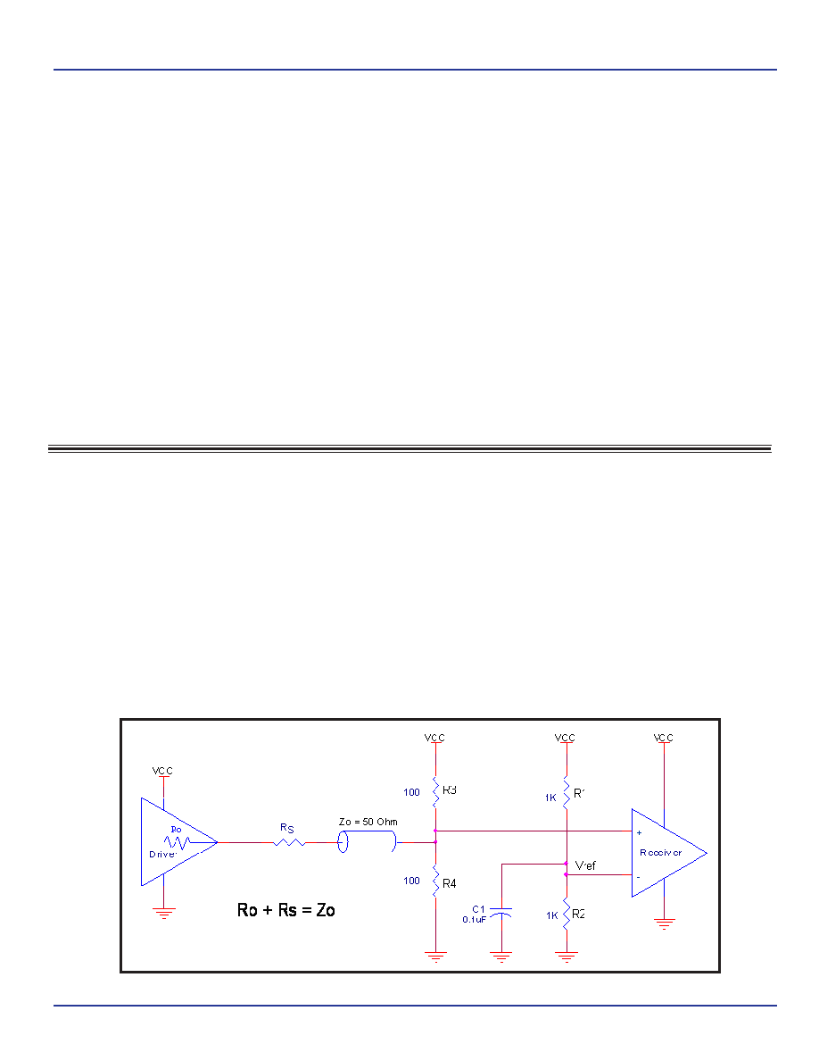
Figure 2 shows how a differential input can be wired to accept
single ended levels. The reference voltage VREF = VDD/2 is
generated by the bias resistors R1 and R2. The bypass capacitor
(C1) is used to help filter noise on the DC bias. This bias circuit
should be located as close to the input pin as possible. The ratio
of R1 and R2 might need to be adjusted to position the VREF in the
center of the input voltage swing. For example, if the input clock
swing is 2.5V and VDD = 3.3V, R1 and R2 value should be adjusted
to set VREF at 1.25V. The values below are for when both the single-
ended swing and VDD are at the same voltage. This configuration
requires that the sum of the output impedance of the driver (Ro)
and the series resistance (Rs) equals the transmission line
impedance. In addition, matched termination at the input will
attenuate the signal in half. This can be done in one of two ways.
First, R3 and R4 in parallel should equal the transmission line
FIGURE 2. SINGLE ENDED SIGNAL DRIVING DIFFERENTIAL INPUT
WIRING THE DIFFERENTIAL INPUT TO ACCEPT SINGLE ENDED LEVELS
impedance. For most 50 applications, R3 and R4 can be 100
Ω.
The values of the resistors can be increased to reduce the loading
for slower and weaker LVCMOS driver. When using single ended
signaling, the noise rejection benefits of differential signaling are
reduced. Even though the differential input can handle full rail
LVCMOS signaling, it is recommended that the amplitude be
reduced. The datasheet specifies a lower differential amplitude,
however this only applies to differential signals. For single-ended
applications, the swing can be larger, however V
IL cannot be less
than -0.3V and VIH cannot be more than VDD + 0.3V. Though some
of the recommended components might not be used, the pads
should be placed in the layout. They can be utilized for debugging
purposes. The datasheet specifications are characterized and
guaranteed by using a differential signal.
相关PDF资料 |
PDF描述 |
|---|---|
| ICS85105AGILF | IC CLOCK BUFFER MUX 2:5 20-TSSOP |
| ICS85108AGILFT | IC CLK BUFFER 1:8 500MHZ 24TSSOP |
| ICS8516FYILFT | IC CLK BUFF 1:16 700MHZ 48-LQFP |
| ICS8516FYLFT | IC CLK BUFF 1:16 700MHZ 48-LQFP |
| ICS8520DYLF | IC CLK BUFF 1:16 500MHZ 48-LQFP |
相关代理商/技术参数 |
参数描述 |
|---|---|
| ICS85105AGI | 制造商:Integrated Device Technology Inc 功能描述:IC CLK BUFFER 2:5 500MHZ 20TSSOP |
| ICS85105AGILF | 功能描述:IC CLOCK BUFFER MUX 2:5 20-TSSOP RoHS:是 类别:集成电路 (IC) >> 时钟/计时 - 时钟缓冲器,驱动器 系列:HiPerClockS™ 标准包装:74 系列:- 类型:扇出缓冲器(分配) 电路数:1 比率 - 输入:输出:1:10 差分 - 输入:输出:是/是 输入:HCSL, LVCMOS, LVDS, LVPECL, LVTTL 输出:HCSL,LVDS 频率 - 最大:400MHz 电源电压:3 V ~ 3.6 V 工作温度:-40°C ~ 85°C 安装类型:表面贴装 封装/外壳:32-VFQFN 裸露焊盘 供应商设备封装:32-QFN(5x5) 包装:管件 |
| ICS85105AGILFT | 功能描述:IC CLOCK BUFFER MUX 2:5 20-TSSOP RoHS:是 类别:集成电路 (IC) >> 时钟/计时 - 时钟缓冲器,驱动器 系列:HiPerClockS™ 标准包装:74 系列:- 类型:扇出缓冲器(分配) 电路数:1 比率 - 输入:输出:1:10 差分 - 输入:输出:是/是 输入:HCSL, LVCMOS, LVDS, LVPECL, LVTTL 输出:HCSL,LVDS 频率 - 最大:400MHz 电源电压:3 V ~ 3.6 V 工作温度:-40°C ~ 85°C 安装类型:表面贴装 封装/外壳:32-VFQFN 裸露焊盘 供应商设备封装:32-QFN(5x5) 包装:管件 |
| ICS85105AGIT | 制造商:Integrated Device Technology Inc 功能描述:IC CLK BUFFER 2:5 500MHZ 20TSSOP |
| ICS85108AGI | 制造商:Integrated Device Technology Inc 功能描述:IC CLK BUFFER 1:8 500MHZ 24TSSOP |
发布紧急采购,3分钟左右您将得到回复。