- 您现在的位置:买卖IC网 > PDF目录67697 > ICS8534AY-01LF (INTEGRATED DEVICE TECHNOLOGY INC) 8534 SERIES, LOW SKEW CLOCK DRIVER, 22 TRUE OUTPUT(S), 0 INVERTED OUTPUT(S), PQFP64 PDF资料下载
参数资料
| 型号: | ICS8534AY-01LF |
| 厂商: | INTEGRATED DEVICE TECHNOLOGY INC |
| 元件分类: | 时钟及定时 |
| 英文描述: | 8534 SERIES, LOW SKEW CLOCK DRIVER, 22 TRUE OUTPUT(S), 0 INVERTED OUTPUT(S), PQFP64 |
| 封装: | 10 X 10 MM, 1 MM HEIGHT, MS-026, TQFP-64 |
| 文件页数: | 5/20页 |
| 文件大小: | 1733K |
| 代理商: | ICS8534AY-01LF |
ICS8534-01
LOW SKEW, 1-TO-22 DIFFERENTIAL-TO-3.3V LVPECL FANOUT BUFFER
IDT / ICS 3.3V LVPECL FANOUT BUFFER
13
ICS8534AY-01 REV. A DECEMBER 6, 2007
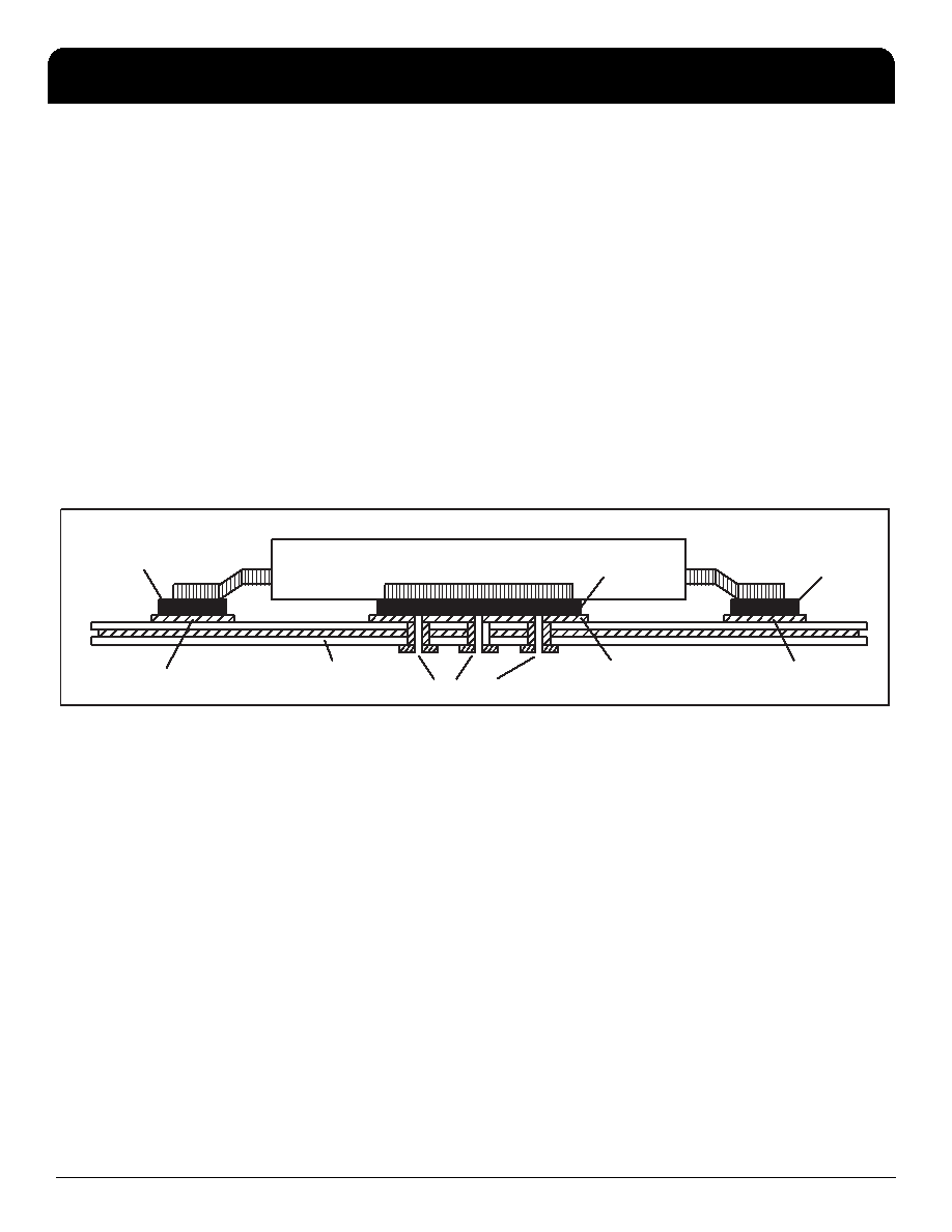
EPAD Thermal Release Path
In order to maximize both the removal of heat from the package
and the electrical performance, a land pattern must be
incorporated on the Printed Circuit Board (PCB) within the footprint
of the package corresponding to the exposed metal pad or
exposed heat slug on the package, as shown in Figure 6. The
solderable area on the PCB, as defined by the solder mask, should
be at least the same size/shape as the exposed pad/slug area on
the package to maximize the thermal/electrical performance.
Sufficient clearance should be designed on the PCB between the
outer edges of the land pattern and the inner edges of pad pattern
for the leads to avoid any shorts.
While the land pattern on the PCB provides a means of heat
transfer and electrical grounding from the package to the board
through a solder joint, thermal vias are necessary to effectively
conduct from the surface of the PCB to the ground plane(s). The
land pattern must be connected to ground through these vias. The
vias act as “heat pipes”. The number of vias (i.e. “heat pipes”) are
application specific and dependent upon the package power
dissipation as well as electrical conductivity requirements. Thus,
thermal and electrical analysis and/or testing are recommended to
determine the minimum number needed. Maximum thermal and
electrical performance is achieved when an array of vias is
incorporated in the land pattern. It is recommended to use as many
vias connected to ground as possible. It is also recommended that
the via diameter should be 12 to 13mils (0.30 to 0.33mm) with 1oz
copper via barrel plating. This is desirable to avoid any solder
wicking inside the via during the soldering process which may
result in voids in solder between the exposed pad/slug and the
thermal land. Precautions should be taken to eliminate any solder
voids between the exposed heat slug and the land pattern. Note:
These recommendations are to be used as a guideline only. For
further information, refer to the Application Note on the Surface
Mount Assembly of Amkor’s Thermally/Electrically Enhance
Leadfame Base Package, Amkor Technology.
Figure 6. Assembly for Exposed Pad Thermal Release Path - Side View (drawing not to scale)
GROUND PLANE
LAND PATTERN
SOLDER
THERMAL VIA
EXPOSED HEAT SLUG
(GROUND PAD)
PIN
PIN PAD
SOLDER
PIN
PIN PAD
SOLDER
相关PDF资料 |
PDF描述 |
|---|---|
| ICS8534BMI-13LFT | 266 MHz, OTHER CLOCK GENERATOR, PDSO16 |
| ICS8534BMI-13T | 266 MHz, OTHER CLOCK GENERATOR, PDSO16 |
| ICS8534BMI-13 | 266 MHz, OTHER CLOCK GENERATOR, PDSO16 |
| ICS85352AYILFT | 85352 SERIES, LOW SKEW CLOCK DRIVER, 12 TRUE OUTPUT(S), 0 INVERTED OUTPUT(S), PQFP48 |
| ICS85354AK-01 | 85354 SERIES, 2 LINE TO 1 LINE MULTIPLEXER, COMPLEMENTARY OUTPUT, QCC16 |
相关代理商/技术参数 |
参数描述 |
|---|---|
| ICS8534AY-01LFT | 功能描述:IC CLOCK BUFFER MUX 2:22 64-TQFP RoHS:是 类别:集成电路 (IC) >> 时钟/计时 - 时钟缓冲器,驱动器 系列:HiPerClockS™ 标准包装:74 系列:- 类型:扇出缓冲器(分配) 电路数:1 比率 - 输入:输出:1:10 差分 - 输入:输出:是/是 输入:HCSL, LVCMOS, LVDS, LVPECL, LVTTL 输出:HCSL,LVDS 频率 - 最大:400MHz 电源电压:3 V ~ 3.6 V 工作温度:-40°C ~ 85°C 安装类型:表面贴装 封装/外壳:32-VFQFN 裸露焊盘 供应商设备封装:32-QFN(5x5) 包装:管件 |
| ICS8534BMI-13LF | 功能描述:IC CLOCK BUFFER MUX 2:4 16-SOIC RoHS:是 类别:集成电路 (IC) >> 时钟/计时 - 时钟缓冲器,驱动器 系列:HiPerClockS™ 标准包装:74 系列:- 类型:扇出缓冲器(分配) 电路数:1 比率 - 输入:输出:1:10 差分 - 输入:输出:是/是 输入:HCSL, LVCMOS, LVDS, LVPECL, LVTTL 输出:HCSL,LVDS 频率 - 最大:400MHz 电源电压:3 V ~ 3.6 V 工作温度:-40°C ~ 85°C 安装类型:表面贴装 封装/外壳:32-VFQFN 裸露焊盘 供应商设备封装:32-QFN(5x5) 包装:管件 |
| ICS8534BMI-13LFT | 功能描述:IC CLOCK BUFFER MUX 2:4 16-SOIC RoHS:是 类别:集成电路 (IC) >> 时钟/计时 - 时钟缓冲器,驱动器 系列:HiPerClockS™ 标准包装:74 系列:- 类型:扇出缓冲器(分配) 电路数:1 比率 - 输入:输出:1:10 差分 - 输入:输出:是/是 输入:HCSL, LVCMOS, LVDS, LVPECL, LVTTL 输出:HCSL,LVDS 频率 - 最大:400MHz 电源电压:3 V ~ 3.6 V 工作温度:-40°C ~ 85°C 安装类型:表面贴装 封装/外壳:32-VFQFN 裸露焊盘 供应商设备封装:32-QFN(5x5) 包装:管件 |
| ICS85352AYILF | 功能描述:IC CLOCK MUX 2:12 700MHZ 48-TQFP RoHS:是 类别:集成电路 (IC) >> 时钟/计时 - 时钟缓冲器,驱动器 系列:HiPerClockS™ 产品培训模块:High Bandwidth Product Overview 标准包装:1,000 系列:Precision Edge® 类型:扇出缓冲器(分配) 电路数:1 比率 - 输入:输出:1:4 差分 - 输入:输出:是/是 输入:CML,LVDS,LVPECL 输出:CML 频率 - 最大:2.5GHz 电源电压:2.375 V ~ 2.625 V 工作温度:-40°C ~ 85°C 安装类型:表面贴装 封装/外壳:16-VFQFN 裸露焊盘,16-MLF? 供应商设备封装:16-MLF?(3x3) 包装:带卷 (TR) |
| ICS85352AYILFT | 功能描述:IC CLOCK MUX 2:12 700MHZ 48-TQFP RoHS:是 类别:集成电路 (IC) >> 时钟/计时 - 时钟缓冲器,驱动器 系列:HiPerClockS™ 标准包装:74 系列:- 类型:扇出缓冲器(分配) 电路数:1 比率 - 输入:输出:1:10 差分 - 输入:输出:是/是 输入:HCSL, LVCMOS, LVDS, LVPECL, LVTTL 输出:HCSL,LVDS 频率 - 最大:400MHz 电源电压:3 V ~ 3.6 V 工作温度:-40°C ~ 85°C 安装类型:表面贴装 封装/外壳:32-VFQFN 裸露焊盘 供应商设备封装:32-QFN(5x5) 包装:管件 |
发布紧急采购,3分钟左右您将得到回复。