- 您现在的位置:买卖IC网 > PDF目录67699 > ICS8634BK-01 (INTEGRATED DEVICE TECHNOLOGY INC) 8634 SERIES, PLL BASED CLOCK DRIVER, 5 TRUE OUTPUT(S), 0 INVERTED OUTPUT(S), QCC32 PDF资料下载
参数资料
| 型号: | ICS8634BK-01 |
| 厂商: | INTEGRATED DEVICE TECHNOLOGY INC |
| 元件分类: | 时钟及定时 |
| 英文描述: | 8634 SERIES, PLL BASED CLOCK DRIVER, 5 TRUE OUTPUT(S), 0 INVERTED OUTPUT(S), QCC32 |
| 封装: | 5 X 5 MM, 0.95 MM HEIGHT, MO-220, VFQFN-32 |
| 文件页数: | 16/16页 |
| 文件大小: | 246K |
| 代理商: | ICS8634BK-01 |
8634BY-01
www.icst.com/products/hiperclocks.html
REV. D APRIL 12, 2007
9
Integrated
Circuit
Systems, Inc.
ICS8634-01
1-TO-5 DIFFERENTIAL-TO-3.3V LVPECL
ZERO DELAY BUFFER
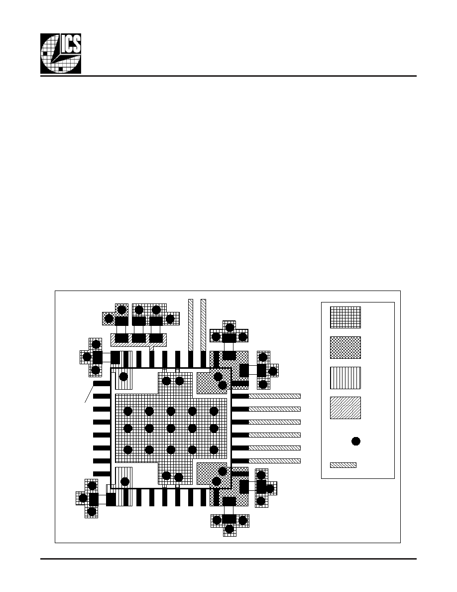
The following component footprints are used in this layout
example:
All the resistors and capacitors are size 0603.
POWER AND GROUNDING
Place the decoupling capacitors C1, C2, C4, C5, C6, and C7, as
close as possible to the power pins. If space allows, placement
of the decoupling capacitor on the component side is preferred.
This can reduce unwanted inductance between the decoupling
capacitor and the power pin caused by the via.
Maximize the power and ground pad sizes and number of vias
capacitors. This can reduce the inductance between the power
and ground planes and the component power and ground pins.
The RC filter consisting of R7, C11, and C16 should be placed
as close to the V
CCA pin as possible.
CLOCK TRACES AND TERMINATION
Poor signal integrity can degrade the system performance or
cause system failure. In synchronous high-speed digital systems,
the clock signal is less tolerant to poor signal integrity than other
signals. Any ringing on the rising or falling edge or excessive ring
back can cause system failure. The shape of the trace and the
trace delay might be restricted by the available space on the board
and the component location. While routing the traces, the clock
signal traces should be routed first and should be locked prior to
routing other signal traces.
The differential 50
Ω output traces should have same
length.
Avoid sharp angles on the clock trace. Sharp angle
turns cause the characteristic impedance to change on
the transmission lines.
Keep the clock traces on the same layer. Whenever pos-
sible, avoid placing vias on the clock traces. Placement
of vias on the traces can affect the trace characteristic
impedance and hence degrade signal integrity.
To prevent cross talk, avoid routing other signal traces in
parallel with the clock traces. If running parallel traces is
unavoidable, allow a separation of at least three trace
widths between the differential clock trace and the other
signal trace.
Make sure no other signal traces are routed between the
clock trace pair.
The matching termination resistors should be located as
close to the receiver input pins as possible.
FIGURE 5B.
PCB BOARD LAYOUT FOR ICS8634-01
C4
C1
U1
VIA
VCCA
VCCO
C7
C11
C16
C5
VCC
C2
C6
GND
R7
50 Ohm
Traces
Pin 1
相关PDF资料 |
PDF描述 |
|---|---|
| ICS8634BY-01LF | 8634 SERIES, PLL BASED CLOCK DRIVER, 5 TRUE OUTPUT(S), 0 INVERTED OUTPUT(S), PQFP32 |
| ICS8634BY-01T | 8634 SERIES, PLL BASED CLOCK DRIVER, 5 TRUE OUTPUT(S), 0 INVERTED OUTPUT(S), PQFP32 |
| ICS8634BK-01T | 8634 SERIES, PLL BASED CLOCK DRIVER, 5 TRUE OUTPUT(S), 0 INVERTED OUTPUT(S), QCC32 |
| ICS86953AYI-147LF | PLL BASED CLOCK DRIVER, 8 TRUE OUTPUT(S), 0 INVERTED OUTPUT(S), PQFP32 |
| ICS86953AYI-147LF | PLL BASED CLOCK DRIVER, 8 TRUE OUTPUT(S), 0 INVERTED OUTPUT(S), PQFP32 |
相关代理商/技术参数 |
参数描述 |
|---|---|
| ICS8634BY-01LF | 功能描述:IC BUFFER ZD 1:5 LVPECL 32-LQFP RoHS:是 类别:集成电路 (IC) >> 时钟/计时 - 时钟发生器,PLL,频率合成器 系列:HiPerClockS™ 标准包装:2,000 系列:- 类型:PLL 频率合成器 PLL:是 输入:晶体 输出:时钟 电路数:1 比率 - 输入:输出:1:1 差分 - 输入:输出:无/无 频率 - 最大:1GHz 除法器/乘法器:是/无 电源电压:4.5 V ~ 5.5 V 工作温度:-20°C ~ 85°C 安装类型:表面贴装 封装/外壳:16-LSSOP(0.175",4.40mm 宽) 供应商设备封装:16-SSOP 包装:带卷 (TR) 其它名称:NJW1504V-TE1-NDNJW1504V-TE1TR |
| ICS8634BY-01LFT | 功能描述:IC BUFFER ZD 1-5 LVPECL 32-LQFP RoHS:是 类别:集成电路 (IC) >> 时钟/计时 - 时钟发生器,PLL,频率合成器 系列:HiPerClockS™ 标准包装:1,000 系列:- 类型:时钟/频率合成器,扇出分配 PLL:- 输入:- 输出:- 电路数:- 比率 - 输入:输出:- 差分 - 输入:输出:- 频率 - 最大:- 除法器/乘法器:- 电源电压:- 工作温度:- 安装类型:表面贴装 封装/外壳:56-VFQFN 裸露焊盘 供应商设备封装:56-VFQFP-EP(8x8) 包装:带卷 (TR) 其它名称:844S012AKI-01LFT |
| ICS864S004AKILF | 功能描述:IC BUFFER ZD LVDS ATTEN 32VFQFPN RoHS:是 类别:集成电路 (IC) >> 时钟/计时 - 时钟发生器,PLL,频率合成器 系列:HiPerClockS™ 标准包装:27 系列:Precision Edge® 类型:频率合成器 PLL:是 输入:PECL,晶体 输出:PECL 电路数:1 比率 - 输入:输出:1:1 差分 - 输入:输出:无/是 频率 - 最大:800MHz 除法器/乘法器:是/无 电源电压:3.135 V ~ 5.25 V 工作温度:0°C ~ 85°C 安装类型:表面贴装 封装/外壳:28-SOIC(0.295",7.50mm 宽) 供应商设备封装:28-SOIC 包装:管件 |
| ICS864S004AKILFT | 功能描述:IC BUFFER ZD LVDS ATTEN 32VFQFPN RoHS:是 类别:集成电路 (IC) >> 时钟/计时 - 时钟发生器,PLL,频率合成器 系列:HiPerClockS™ 标准包装:27 系列:Precision Edge® 类型:频率合成器 PLL:是 输入:PECL,晶体 输出:PECL 电路数:1 比率 - 输入:输出:1:1 差分 - 输入:输出:无/是 频率 - 最大:800MHz 除法器/乘法器:是/无 电源电压:3.135 V ~ 5.25 V 工作温度:0°C ~ 85°C 安装类型:表面贴装 封装/外壳:28-SOIC(0.295",7.50mm 宽) 供应商设备封装:28-SOIC 包装:管件 |
| ICS86962CYI-01 | 功能描述:IC BUFFER ZD LVCMOS/LVTTL 32LQFP RoHS:否 类别:集成电路 (IC) >> 时钟/计时 - 时钟发生器,PLL,频率合成器 系列:HiPerClockS™ 标准包装:1,000 系列:- 类型:时钟/频率合成器,扇出分配 PLL:- 输入:- 输出:- 电路数:- 比率 - 输入:输出:- 差分 - 输入:输出:- 频率 - 最大:- 除法器/乘法器:- 电源电压:- 工作温度:- 安装类型:表面贴装 封装/外壳:56-VFQFN 裸露焊盘 供应商设备封装:56-VFQFP-EP(8x8) 包装:带卷 (TR) 其它名称:844S012AKI-01LFT |
发布紧急采购,3分钟左右您将得到回复。