- 您现在的位置:买卖IC网 > PDF目录1998 > ICS874001AGI-02LF (IDT, Integrated Device Technology Inc)IC PCI EXPRSS/JITT ATTEN 20TSSOP PDF资料下载
参数资料
| 型号: | ICS874001AGI-02LF |
| 厂商: | IDT, Integrated Device Technology Inc |
| 文件页数: | 2/17页 |
| 文件大小: | 0K |
| 描述: | IC PCI EXPRSS/JITT ATTEN 20TSSOP |
| 标准包装: | 74 |
| 系列: | FemtoClock™, PCI Express™ (PCIe) |
| 类型: | 漂移衰减器,多路复用器 |
| PLL: | 是 |
| 主要目的: | PCI Express(PCIe) |
| 输入: | HCSL,LVDS,LVHSTL,LVPECL,SSTL |
| 输出: | LVDS |
| 电路数: | 1 |
| 比率 - 输入:输出: | 1:1 |
| 差分 - 输入:输出: | 是/是 |
| 频率 - 最大: | 640MHz |
| 电源电压: | 2.375 V ~ 3.465 V |
| 工作温度: | -40°C ~ 85°C |
| 安装类型: | 表面贴装 |
| 封装/外壳: | 20-TSSOP(0.173",4.40mm 宽) |
| 供应商设备封装: | 20-TSSOP |
| 包装: | 管件 |
| 其它名称: | ICS874001AGI-02LF-ND |
ICS874001AGI-02 REVISION A AUGUST 30, 2010
10
2010 Integrated Device Technology, Inc.
ICS74001I-02 Data Sheet
PCI EXPRESS JITTER ATTENUATOR
ApplicationS Information
Power Supply Filtering Technique
As in any high speed analog circuitry, the power supply pins are
vulnerable to random noise. To achieve optimum jitter performance,
power supply isolation is required. The ICS874001I-02 provides
separate power supplies to isolate any high switching noise from the
outputs to the internal PLL. VDD, VDDA and VDDO should be
individually connected to the power supply plane through vias, and
0.01F bypass capacitors should be used for each pin. Figure 1
illustrates this for a generic VDD pin and also shows that VDDA
requires that an additional 10
resistor along with a 10F bypass
capacitor be connected to the VDDA pin.
Figure 1. Power Supply Filtering
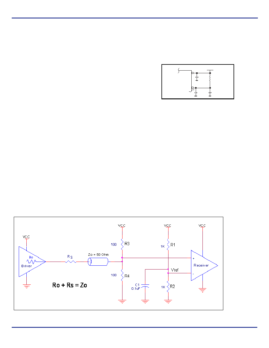
Wiring the Differential Input to Accept Single-Ended Levels
Figure 2 shows how a differential input can be wired to accept single
ended levels. The reference voltage VREF = VDD/2 is generated by
the bias resistors R1 and R2. The bypass capacitor (C1) is used to
help filter noise on the DC bias. This bias circuit should be located as
close to the input pin as possible. The ratio of R1 and R2 might need
to be adjusted to position the VREF in the center of the input voltage
swing. For example, if the input clock swing is 2.5V and VDD = 3.3V,
R1 and R2 value should be adjusted to set VREF at 1.25V. The values
below are for when both the single ended swing and VDD are at the
same voltage. This configuration requires that the sum of the output
impedance of the driver (Ro) and the series resistance (Rs) equals
the transmission line impedance. In addition, matched termination at
the input will attenuate the signal in half. This can be done in one of
two ways. First, R3 and R4 in parallel should equal the transmission
line impedance. For most 50
applications, R3 and R4 can be 100.
The values of the resistors can be increased to reduce the loading for
slower and weaker LVCMOS driver. When using single-ended
signaling, the noise rejection benefits of differential signaling are
reduced. Even though the differential input can handle full rail
LVCMOS signaling, it is recommended that the amplitude be
reduced. The datasheet specifies a lower differential amplitude,
however this only applies to differential signals. For single-ended
applications, the swing can be larger, however VIL cannot be less
than -0.3V and VIH cannot be more than VDD + 0.3V. Though some
of the recommended components might not be used, the pads
should be placed in the layout. They can be utilized for debugging
purposes. The datasheet specifications are characterized and
guaranteed by using a differential signal.
Figure 2. Recommended Schematic for Wiring a Differential Input to Accept Single-ended Levels
VDD
VDDA
3.3V or 2.5V
10
10F
.01F
相关PDF资料 |
PDF描述 |
|---|---|
| ICS874001AGI-05LFT | IC PCI EXPRSS/JITT ATTEN 20TSSOP |
| ICS874002AGLFT | IC PCI EXPRSS/JITT ATTEN 20TSSOP |
| ICS874005AG-04LFT | IC PCI EXPRSS/JITT ATTEN 24TSSOP |
| ICS874005AGLFT | IC PCI EXPRSS/JITT ATTEN 24TSSOP |
| ICS8741004AGLFT | IC PCI EXPRSS/JITT ATTEN 24TSSOP |
相关代理商/技术参数 |
参数描述 |
|---|---|
| ICS874001AGI-02LFT | 功能描述:IC PCI EXPRSS/JITT ATTEN 20TSSOP RoHS:是 类别:集成电路 (IC) >> 时钟/计时 - 专用 系列:FemtoClock™, PCI Express™ (PCIe) 标准包装:1,500 系列:- 类型:时钟缓冲器/驱动器 PLL:是 主要目的:- 输入:- 输出:- 电路数:- 比率 - 输入:输出:- 差分 - 输入:输出:- 频率 - 最大:- 电源电压:3.3V 工作温度:0°C ~ 70°C 安装类型:表面贴装 封装/外壳:28-SSOP(0.209",5.30mm 宽) 供应商设备封装:28-SSOP 包装:带卷 (TR) 其它名称:93786AFT |
| ICS874001AGI-05LF | 功能描述:IC PCI EXPRSS/JITT ATTEN 20TSSOP RoHS:是 类别:集成电路 (IC) >> 时钟/计时 - 专用 系列:FemtoClock™, PCI Express™ (PCIe) 标准包装:1 系列:- 类型:时钟/频率发生器,多路复用器 PLL:是 主要目的:存储器,RDRAM 输入:晶体 输出:LVCMOS 电路数:1 比率 - 输入:输出:1:2 差分 - 输入:输出:无/是 频率 - 最大:400MHz 电源电压:3 V ~ 3.6 V 工作温度:0°C ~ 85°C 安装类型:表面贴装 封装/外壳:16-TSSOP(0.173",4.40mm 宽) 供应商设备封装:16-TSSOP 包装:Digi-Reel® 其它名称:296-6719-6 |
| ICS874001AGI-05LFT | 功能描述:IC PCI EXPRSS/JITT ATTEN 20TSSOP RoHS:是 类别:集成电路 (IC) >> 时钟/计时 - 专用 系列:FemtoClock™, PCI Express™ (PCIe) 标准包装:1,500 系列:- 类型:时钟缓冲器/驱动器 PLL:是 主要目的:- 输入:- 输出:- 电路数:- 比率 - 输入:输出:- 差分 - 输入:输出:- 频率 - 最大:- 电源电压:3.3V 工作温度:0°C ~ 70°C 安装类型:表面贴装 封装/外壳:28-SSOP(0.209",5.30mm 宽) 供应商设备封装:28-SSOP 包装:带卷 (TR) 其它名称:93786AFT |
| ICS874002AGLF | 功能描述:IC JITTER ATTENUATOR 20-TSSOP RoHS:是 类别:集成电路 (IC) >> 时钟/计时 - 专用 系列:HiPerClockS™, PCI Express® (PCIe) 标准包装:1 系列:- 类型:时钟/频率发生器,多路复用器 PLL:是 主要目的:存储器,RDRAM 输入:晶体 输出:LVCMOS 电路数:1 比率 - 输入:输出:1:2 差分 - 输入:输出:无/是 频率 - 最大:400MHz 电源电压:3 V ~ 3.6 V 工作温度:0°C ~ 85°C 安装类型:表面贴装 封装/外壳:16-TSSOP(0.173",4.40mm 宽) 供应商设备封装:16-TSSOP 包装:Digi-Reel® 其它名称:296-6719-6 |
| ICS874002AGLFT | 功能描述:IC PCI EXPRSS/JITT ATTEN 20TSSOP RoHS:是 类别:集成电路 (IC) >> 时钟/计时 - 专用 系列:HiPerClockS™, PCI Express® (PCIe) 标准包装:1,500 系列:- 类型:时钟缓冲器/驱动器 PLL:是 主要目的:- 输入:- 输出:- 电路数:- 比率 - 输入:输出:- 差分 - 输入:输出:- 频率 - 最大:- 电源电压:3.3V 工作温度:0°C ~ 70°C 安装类型:表面贴装 封装/外壳:28-SSOP(0.209",5.30mm 宽) 供应商设备封装:28-SSOP 包装:带卷 (TR) 其它名称:93786AFT |
发布紧急采购,3分钟左右您将得到回复。