- 您现在的位置:买卖IC网 > PDF目录67703 > ICS8745BM-21LF (INTEGRATED DEVICE TECHNOLOGY INC) 8745 SERIES, PLL BASED CLOCK DRIVER, 1 TRUE OUTPUT(S), 0 INVERTED OUTPUT(S), PDSO20 PDF资料下载
参数资料
| 型号: | ICS8745BM-21LF |
| 厂商: | INTEGRATED DEVICE TECHNOLOGY INC |
| 元件分类: | 时钟及定时 |
| 英文描述: | 8745 SERIES, PLL BASED CLOCK DRIVER, 1 TRUE OUTPUT(S), 0 INVERTED OUTPUT(S), PDSO20 |
| 封装: | 7.50 X 12.80 MM, 2.30 MM HEIGHT, ROHS COMPLIANT, MS-013, MO-119, SOIC-20 |
| 文件页数: | 2/19页 |
| 文件大小: | 840K |
| 代理商: | ICS8745BM-21LF |
ICS8745B-21
1:1 DIFFERENTIAL-TO-LVDS ZERO DELAY CLOCK GENERATOR
IDT / ICS LVDS ZERO DELAY CLOCK GENERATOR
10
ICS8745BM-21REV. C APRIL 17, 2007
Application Information
Power Supply Filtering Technique
As in any high speed analog circuitry, the power supply pins are
vulnerable to random noise. The ICS8745B-21 provides separate
power supplies to isolate any high switching noise from the outputs
to the internal PLL. VDD, VDDA and VDDO should be individually
connected to the power supply plane through vias, and bypass
capacitors should be used for each pin. To achieve optimum jitter
performance, power supply isolation is required. Figure 1
illustrates how a 10Ω resistor along with a 10μF and a .01μF
bypass capacitor should be connected to each VDDA pin. The 10Ω
resistor can also be replaced by a ferrite bead.
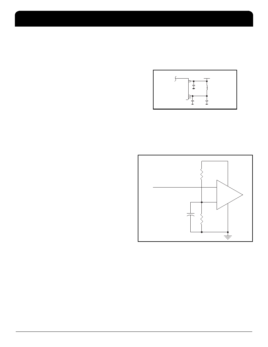
Figure 1. Power Supply Filtering
Wiring the Differential Input to Accept Single Ended Levels
Figure 2 shows how the differential input can be wired to accept
single ended levels. The reference voltage V_REF = VDD/2 is
generated by the bias resistors R1, R2 and C1. This bias circuit
should be located as close as possible to the input pin. The ratio of
R1 and R2 might need to be adjusted to position the V_REF in the
center of the input voltage swing. For example, if the input clock
swing is only 2.5V and VDD = 3.3V, V_REF should be 1.25V and
R2/R1 = 0.609.
Figure 2. Single-Ended Signal Driving Differential Input
VDD
VDDA
3.3V
10
Ω
10F
.01F
V_REF
Single Ended Clock Input
VDD
CLK
nCLK
R1
1K
C1
0.1u
R2
1K
相关PDF资料 |
PDF描述 |
|---|---|
| ICS8745BM-21T | 8745 SERIES, PLL BASED CLOCK DRIVER, 1 TRUE OUTPUT(S), 0 INVERTED OUTPUT(S), PDSO20 |
| ICS8745BMI-21LF | 8745 SERIES, PLL BASED CLOCK DRIVER, 1 TRUE OUTPUT(S), 0 INVERTED OUTPUT(S), PDSO20 |
| ICS8745BMI-21 | 8745 SERIES, PLL BASED CLOCK DRIVER, 1 TRUE OUTPUT(S), 0 INVERTED OUTPUT(S), PDSO20 |
| ICS8745BMI-21LF | PLL BASED CLOCK DRIVER, 1 TRUE OUTPUT(S), 0 INVERTED OUTPUT(S), PDSO20 |
| ICS8745BMI-21 | PLL BASED CLOCK DRIVER, 1 TRUE OUTPUT(S), 0 INVERTED OUTPUT(S), PDSO20 |
相关代理商/技术参数 |
参数描述 |
|---|---|
| ICS8745BM-21LFT | 功能描述:IC CLK GEN 1:1 DIFF-LVDS 20-SOIC RoHS:是 类别:集成电路 (IC) >> 时钟/计时 - 时钟发生器,PLL,频率合成器 系列:HiPerClockS™ 标准包装:1,000 系列:- 类型:时钟/频率合成器,扇出分配 PLL:- 输入:- 输出:- 电路数:- 比率 - 输入:输出:- 差分 - 输入:输出:- 频率 - 最大:- 除法器/乘法器:- 电源电压:- 工作温度:- 安装类型:表面贴装 封装/外壳:56-VFQFN 裸露焊盘 供应商设备封装:56-VFQFP-EP(8x8) 包装:带卷 (TR) 其它名称:844S012AKI-01LFT |
| ICS8745BMI-21LF | 功能描述:IC CLK GEN 1:1 DIFF-LVDS 20-SOIC RoHS:是 类别:集成电路 (IC) >> 时钟/计时 - 时钟发生器,PLL,频率合成器 系列:HiPerClockS™ 标准包装:1,000 系列:Precision Edge® 类型:时钟/频率合成器 PLL:无 输入:CML,PECL 输出:CML 电路数:1 比率 - 输入:输出:2:1 差分 - 输入:输出:是/是 频率 - 最大:10.7GHz 除法器/乘法器:无/无 电源电压:2.375 V ~ 3.6 V 工作温度:-40°C ~ 85°C 安装类型:表面贴装 封装/外壳:16-VFQFN 裸露焊盘,16-MLF? 供应商设备封装:16-MLF?(3x3) 包装:带卷 (TR) 其它名称:SY58052UMGTRSY58052UMGTR-ND |
| ICS8745BMI-21LFT | 功能描述:IC CLK GEN 1:1 DIFF-LVDS 20-SOIC RoHS:是 类别:集成电路 (IC) >> 时钟/计时 - 时钟发生器,PLL,频率合成器 系列:HiPerClockS™ 标准包装:1,000 系列:- 类型:时钟/频率合成器,扇出分配 PLL:- 输入:- 输出:- 电路数:- 比率 - 输入:输出:- 差分 - 输入:输出:- 频率 - 最大:- 除法器/乘法器:- 电源电压:- 工作温度:- 安装类型:表面贴装 封装/外壳:56-VFQFN 裸露焊盘 供应商设备封装:56-VFQFP-EP(8x8) 包装:带卷 (TR) 其它名称:844S012AKI-01LFT |
| ICS8745BY | 制造商:ICS 功能描述: 制造商:Integrated Device Technology Inc 功能描述: 制造商:Integrated Device Technology Inc 功能描述:8745 SERIES, PLL BASED CLOCK DRIVER, 5 TRUE OUTPUT(S), 0 INVERTED OUTPUT(S), PQFP32 |
| ICS8745BYI | 制造商:Integrated Device Technology Inc 功能描述: |
发布紧急采购,3分钟左右您将得到回复。