- 您现在的位置:买卖IC网 > PDF目录65534 > ICS9112YF-17-T (INTEGRATED DEVICE TECHNOLOGY INC) PLL BASED CLOCK DRIVER, 8 TRUE OUTPUT(S), 0 INVERTED OUTPUT(S), PDSO16 PDF资料下载
参数资料
| 型号: | ICS9112YF-17-T |
| 厂商: | INTEGRATED DEVICE TECHNOLOGY INC |
| 元件分类: | 时钟及定时 |
| 英文描述: | PLL BASED CLOCK DRIVER, 8 TRUE OUTPUT(S), 0 INVERTED OUTPUT(S), PDSO16 |
| 封装: | 0.150 INCH, MO-137, SSOP-16 |
| 文件页数: | 3/8页 |
| 文件大小: | 108K |
| 代理商: | ICS9112YF-17-T |
3
ICS9112-17
0051J—02/05/04
Absolute Maximum Ratings
Supply Voltage . . . . . . . . . . . . . . . . . . . . . . . 7.0 V
Logic Inputs . . . . . . . . . . . . . . . . . . . . . . . . . GND –0.5 V to VDD +0.5 V
Ambient Operating Temperature . . . . . . . . . . 0°C to +70°C
Storage Temperature . . . . . . . . . . . . . . . . . . . –65°C to +150°C
Stresses above those listed under
Absolute Maximum Ratings may cause permanent damage to the device. These
ratings are stress specifications only and functional operation of the device at these or any other conditions above those
listed in the operational sections of the specifications is not implied. Exposure to absolute maximum rating conditions
for extended periods may affect product reliability.
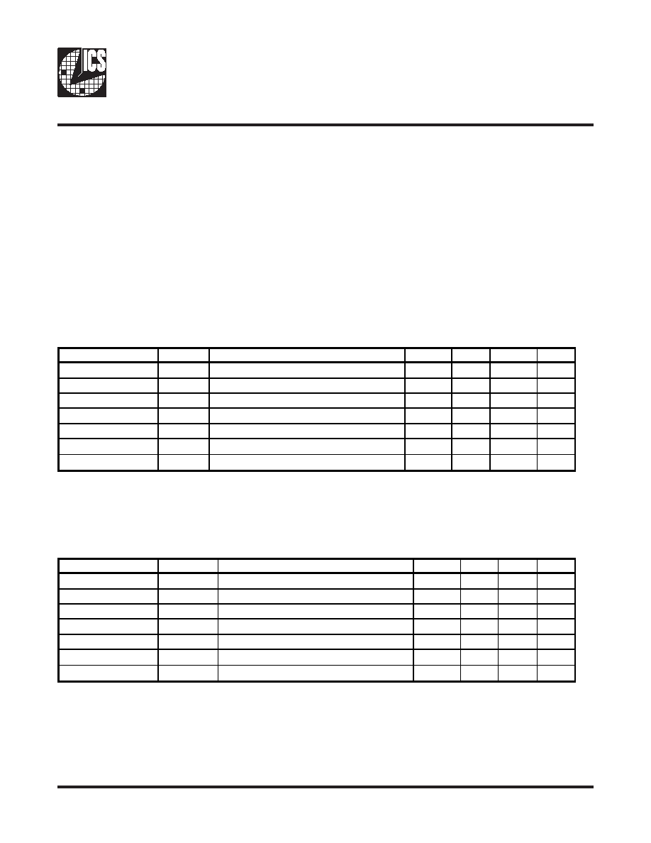
Electrical Characteristics - Input & Supply
TA = 0 - 70C; Supply Voltage VDD = 5.0 V +/-10% (unless otherwise stated)
PARAMETER
SYMBOL
CONDITIONS
MIN
TYP
MAX
UNITS
Input High Voltage
VIH
2.0
2.5
VDD +0.5
V
Input Low Voltage
VIL
GND -0.5
0.8
V
Input High Current
IIH
VIN = VDD
0.1
100
uA
Input Low Current
IIL
VIN = 0 V;
19
50
uA
Operating current
IDD1
CL = 0 pF; FIN @ 66M
45
65
mA
Input frequency
Fi
1
VDD = 3.3 V; All Outputs Loaded
25
133
MHz
Input Capacitance
CIN
1
Logic Inputs
5
pF
1 Guaranteed by design, not 100% tested in production.
Electrical Characteristics - Input & Supply
TA = 0 - 70C; Supply Voltage VDD = 3.3 V +/-10% (unless otherwise stated)
PARAMETER
SYMBOL
CONDITIONS
MIN
TYP
MAX
UNITS
Input High Voltage
VIH
2.0
VDD+0.3
V
Input Low Voltage
VIL
GND-0.3
0.8
V
Input High Current
IIH
VIN = VDD
0.1
100
uA
Input Low Current
IIL
VIN = 0 V;
19
50
uA
Operating current
IDD1
CL = 0 pF; FIN @ 66M
30
45
mA
Input frequency
Fi
1
VDD = 3.3 V; All Outputs Loaded
25
133
MHz
Input Capacitance
CIN
1
Logic Inputs
5.0
pF
1Guarenteed by design, not 100% tested in production.
相关PDF资料 |
PDF描述 |
|---|---|
| ICS9112YM-26LF-T | LOW SKEW CLOCK DRIVER, 4 TRUE OUTPUT(S), 0 INVERTED OUTPUT(S), PDSO8 |
| ICS9112YM-26LFT | 9112 SERIES, LOW SKEW CLOCK DRIVER, 4 TRUE OUTPUT(S), 0 INVERTED OUTPUT(S), PDSO8 |
| ICS9112YM-28LF-T | 9112 SERIES, LOW SKEW CLOCK DRIVER, 5 TRUE OUTPUT(S), 0 INVERTED OUTPUT(S), PDSO8 |
| ICS9112YM-28LF-T | 9112 SERIES, LOW SKEW CLOCK DRIVER, 5 TRUE OUTPUT(S), 0 INVERTED OUTPUT(S), PDSO8 |
| ICS9117M-01LF | 114 MHz, OTHER CLOCK GENERATOR, PDSO8 |
相关代理商/技术参数 |
参数描述 |
|---|---|
| ICS9112YG-16-T | 制造商:ICS 制造商全称:ICS 功能描述:Low Skew Output Buffer |
| ICS9112YG-26-T | 制造商:ICS 制造商全称:ICS 功能描述:Low Skew Output Buffer |
| ICS9112YM-17-T | 制造商:ICS 制造商全称:ICS 功能描述:Low Skew Output Buffer |
| ICS9112YM-27-T | 制造商:ICS 制造商全称:ICS 功能描述:Low Skew PCI / PCI-X Buffer |
| ICS9112YM-28LF-T | 制造商:ICS 制造商全称:ICS 功能描述:Low Skew Output Buffer |
发布紧急采购,3分钟左右您将得到回复。